


Why Many 65W GaN Chargers Cannot Sustain Full Power Output
 18 May,2026
The Engineering Reality Behind "Peak" vs. "Sustained" Performance
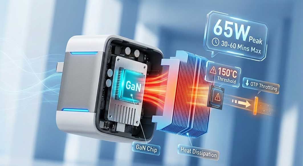
For product engineers and sourcing managers, the "65W" specification on a GaN charger datasheet is often misinterpreted as a continuous capability. In reality, this figure represents a peak power rating. A significant percentage of commercially available compact chargers cannot maintain 65W output for durations exceeding 30 to 60 minutes.
The core engineering challenge lies in the trade-off between power density and thermal dissipation. While Gallium Nitride (GaN) transistors significantly reduce switching losses compared to legacy Silicon (Si) counterparts, they do not eliminate heat generation entirely. As form factors shrink to meet market demand for ultra-portable devices, the surface area available for heat dissipation decreases, leading to rapid internal temperature spikes. When the internal junction temperature approaches the safety threshold—typically around 125°C to 150°C for power components—the controller’s Over-Temperature Protection (OTP) logic engages, forcibly throttling the power output to prevent catastrophic failure.
Technical Breakdown: Thermal Throttling Mechanisms
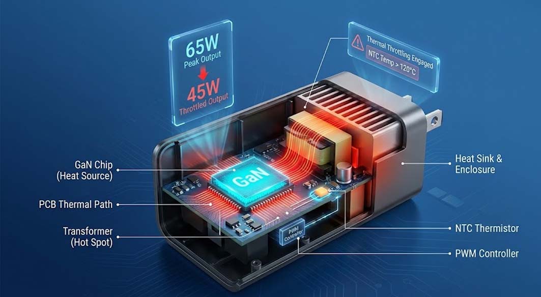
The inability to sustain full power is rarely due to the GaN FETs themselves, which operate efficiently at high frequencies. Instead, the limitation stems from the thermal resistance of the surrounding system, including the PCB layout, transformer core losses, and the enclosure material.
In a 65W GaN charger operating at 94% efficiency, approximately 4W of energy is dissipated as heat . In a standard adapter casing (approx. 50-70cc volume), dissipating 4W without active cooling (fans) relies entirely on conduction and natural convection. If the thermal path is inefficient, heat accumulates in "hot spots"—usually the transformer or the bridge rectifier.
To protect the device, the PWM controller monitors the NTC (Negative Temperature Coefficient) thermistor. Once the detected temperature breaches the pre-set limit (e.g., 90°C chassis temp or 120°C component temp), the controller reduces the current limit or duty cycle. This results in the charger "derating" to a lower profile, often dropping from 65W (20V/3.25A) to 45W (15V/3A) or even 30W.
Comparative Analysis: Thermal Architectures
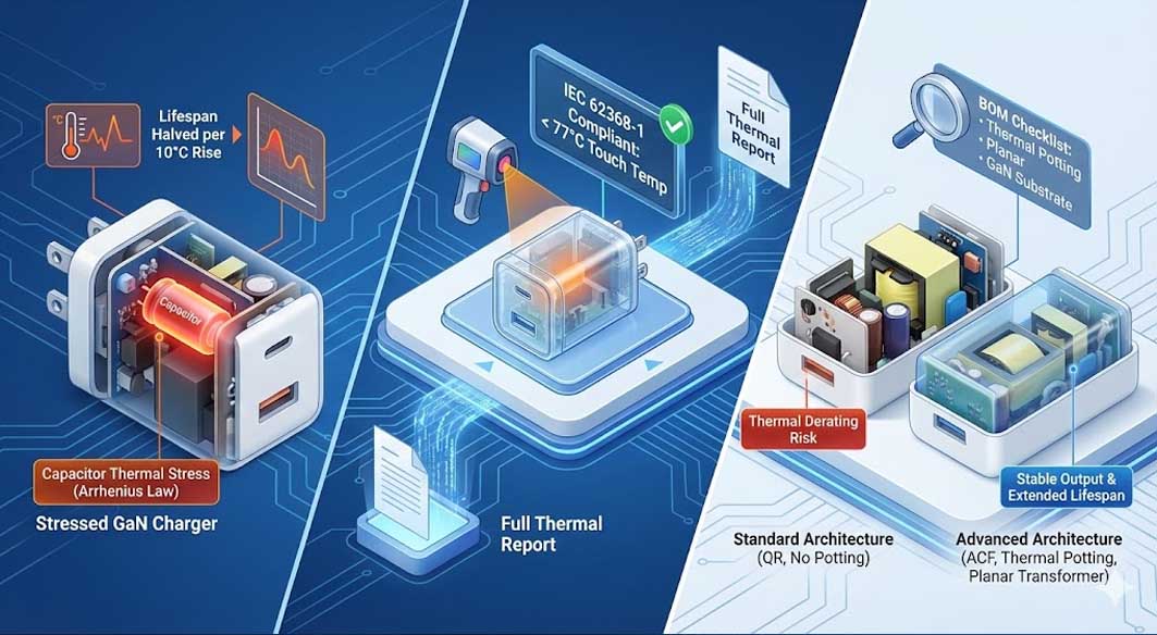
The following table compares the thermal behavior of three common 65W charger architectures under a continuous 1-hour full-load stress test at 25°C ambient temperature.
| Architecture Type | Thermal Strategy | 1-Hour Sustained Output | Max Surface Temp (IEC 62368-1) | Engineering Trade-off |
| Standard GaN (Open Frame) | Air gap insulation; basic thermal pads. | Drops to 45W after ~20 mins | High (>75°C) | Low BOM cost; poor heat transfer from components to case. |
| Fully Potted GaN (Glue Fill) | High-thermal-conductivity potting compound fills all voids. | Maintains 65W (Full Duration) | Moderate (60-65°C) | Higher manufacturing complexity; unrepairable; higher weight. |
| Hybrid Planar Transformer | Flat PCB windings spread heat; integrated heatsinks. | Maintains 65W (Full Duration) | Low (<60°C) | High PCB cost; requires precision automated assembly. |
As indicated, the use of potting compounds (thermal glue) is the critical differentiator for sustaining high power density. By displacing air (which acts as a thermal insulator) with a conductive compound, heat is evenly distributed to the entire surface of the charger casing, preventing localized hot spots that trigger OTP.
Practical Implications for Procurement and QA
For B2B buyers, understanding the distinction between peak and sustained power is critical for supply chain verification. A charger that throttles aggressively may fail to charge larger devices, such as laptops, while they are in use, leading to poor user experience and potential returns.
1. Reliability and Component Lifespan
Thermal cycling—repeated heating and cooling—is the primary cause of fatigue in solder joints and electrolytic capacitors. A 65W GaN charger that constantly hits its thermal limit and throttles will subject its output capacitors to excessive thermal stress. For every 10°C rise in operating temperature, the lifespan of an electrolytic capacitor is roughly halved (Arrhenius Law).
2. Compliance and Safety Standards
IEC 62368-1 imposes strict limits on the touch temperature of consumer electronics (typically 77°C for plastic enclosures). Manufacturers attempting to cut costs by omitting thermal potting often skirt these limits. Sourcing managers should request full thermal reports (thermal imaging data) rather than just electrical efficiency graphs.
3. Evaluating Architecture
When reviewing Bills of Materials (BOM) or structural diagrams, look for references to "thermal potting," "planar transformers," or "GaN-on-Si" vs. "GaN-on-Sapphire" substrates. While sourcing teams must navigate complex specifications, a foundational understanding of everything you need to know about modern phone chargers—specifically regarding topology choices like ACF (Active Clamp Flyback) versus QR (Quasi-Resonant)—helps in predicting which units will suffer from thermal derating before physical testing even begins.
Key Takeaways for Sourcing Managers
Derating is Common: Assume a compact 65W charger will throttle unless thermal potting or advanced planar magnetics are explicitly specified in the design.
Request Burn-in Data: Do not accept instantaneous efficiency metrics. Require a 60-minute full-load burn-in report to verify the output curve remains flat at 65W.
Thermal Management > GaN Chip: The brand of the GaN controller matters less for sustained power than the physical thermal management system (potting, heatsinks, PCB copper weight).
Efficiency $\neq$ Cool: A 95% efficient charger can still overheat if the volume is too small to dissipate the remaining 5% energy loss effectively.
 What B2B Buyers Should Know Before Ordering Phone Chargers?