


What Is a Fast Charger and How Does It Work?
 09 Feb,2026
In the realm of consumer electronics power delivery, the term pd fast charge is often marketed as a feature of convenience, but for engineering and procurement professionals, it represents a complex orchestration of communication protocols, thermal management, and circuit topology. A fast charger is not simply a power supply that outputs higher wattage; it is an intelligent device capable of negotiating voltage and current levels dynamically with the load (the device being charged).
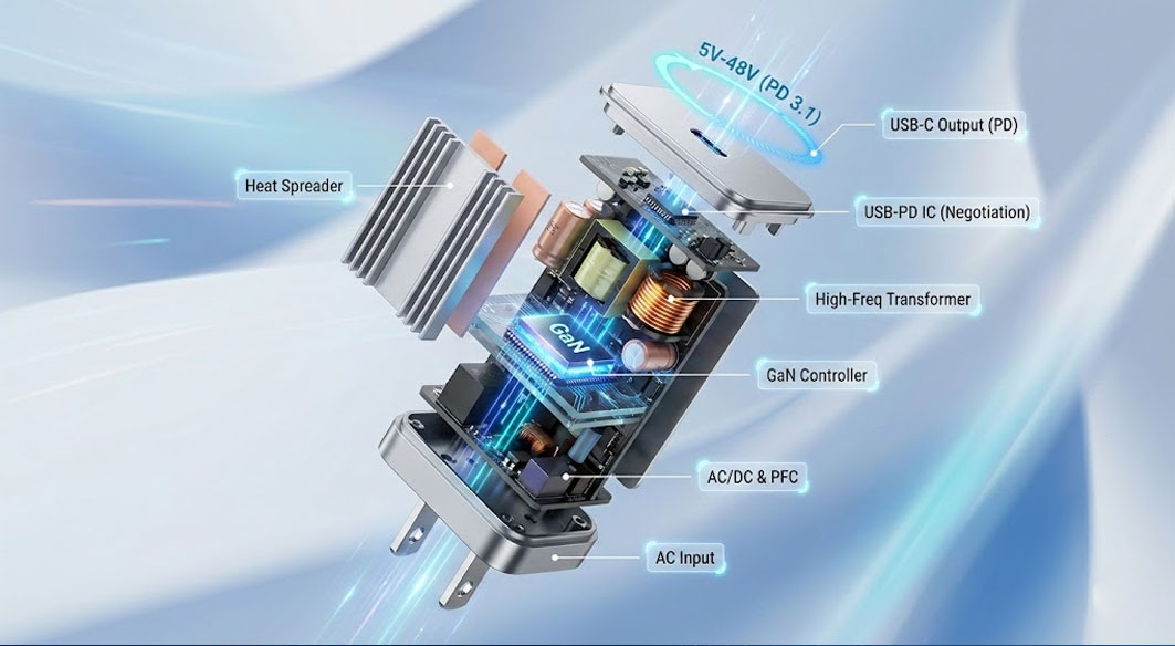
At its core, a pd fast charge system operates by moving beyond the standard 5V/0.5A limits of legacy USB specifications. By utilizing the USB Power Delivery (USB-PD) specification, chargers can deliver variable voltages (ranging from 5V up to 48V in PD 3.1) and higher currents. This capability allows for rapid energy transfer, but it introduces significant challenges in Efficiency, heat dissipation, and electromagnetic interference (EMI) that must be addressed during the design phase.
The Engineering Fundamentals of PD Fast Charge
To understand how a pd fast charge system functions, one must look at the communication logic that occurs the moment a cable is connected. Unlike dumb adaptors that force a constant voltage, a modern pd 3.0 charger engages in a digital "handshake" via the Configuration Channel (CC) pins on the USB-C connector.
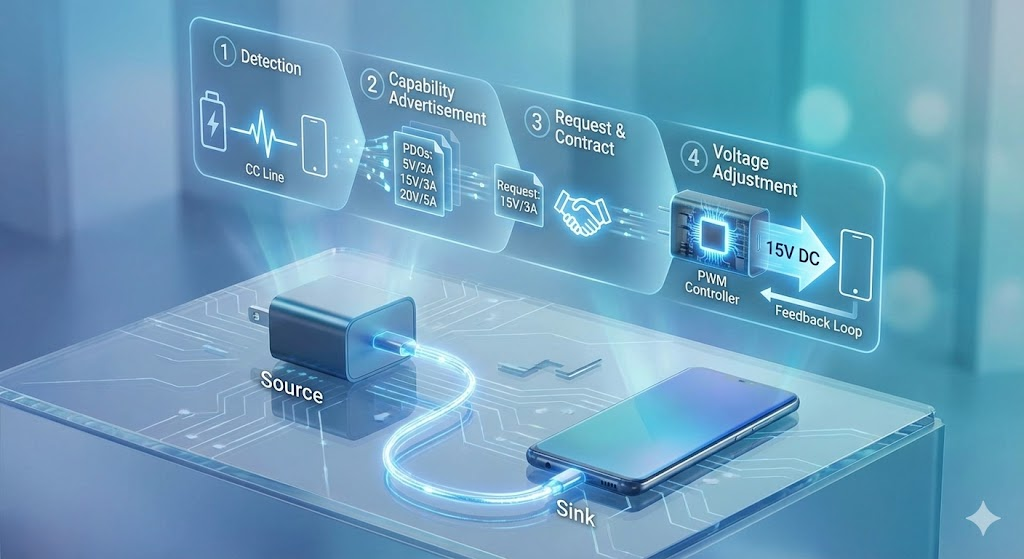
The power delivery process follows a strict engineering sequence:
Detection: The source (charger) detects the presence of a sink (device) via the CC line pull-down resistors.
Capability Advertisement: The source broadcasts its Source Capabilities Data Object (PDO), listing available voltage and current profiles (e.g., 5V/3A, 9V/3A, 15V/3A, 20V/5A).
Request and Contract: The sink requests a specific PDO based on its battery status and thermal headroom. The source accepts, creating an explicit power contract.
Voltage Adjustment: The internal PWM controller adjusts the switching duty cycle to provide the requested voltage.
This negotiation is continuous. If the device battery heats up, it will request a lower power profile to protect the cell, a feature critical for safety but demanding on the charger's feedback loop stability.
Common Industry Pain Points in Charger Development
For OEM buyers and product managers, the specification sheet often hides the realities of mass production. Developing a robust pd 3.0 charger involves mitigating several failure modes that lead to high return rates (RMA).
Key industry challenges include:
Thermal Runaway: High power density in compact enclosures leads to heat accumulation. If the junction temperature of the MOSFETs exceeds 150°C, catastrophic failure occurs.
Audible Noise: Poorly varnished transformers or unstable feedback loops at light loads can cause piezoelectric vibration, resulting in "coil whine."
EMI Compliance: High-frequency switching generates noise. Failing to filter this properly results in failed EMC certifications (FCC/CE), halting shipments.
Vbus Ripple: Excessive voltage ripple can interfere with the touch sensitivity of the connected device’s screen, a common user complaint with low-tier chargers.
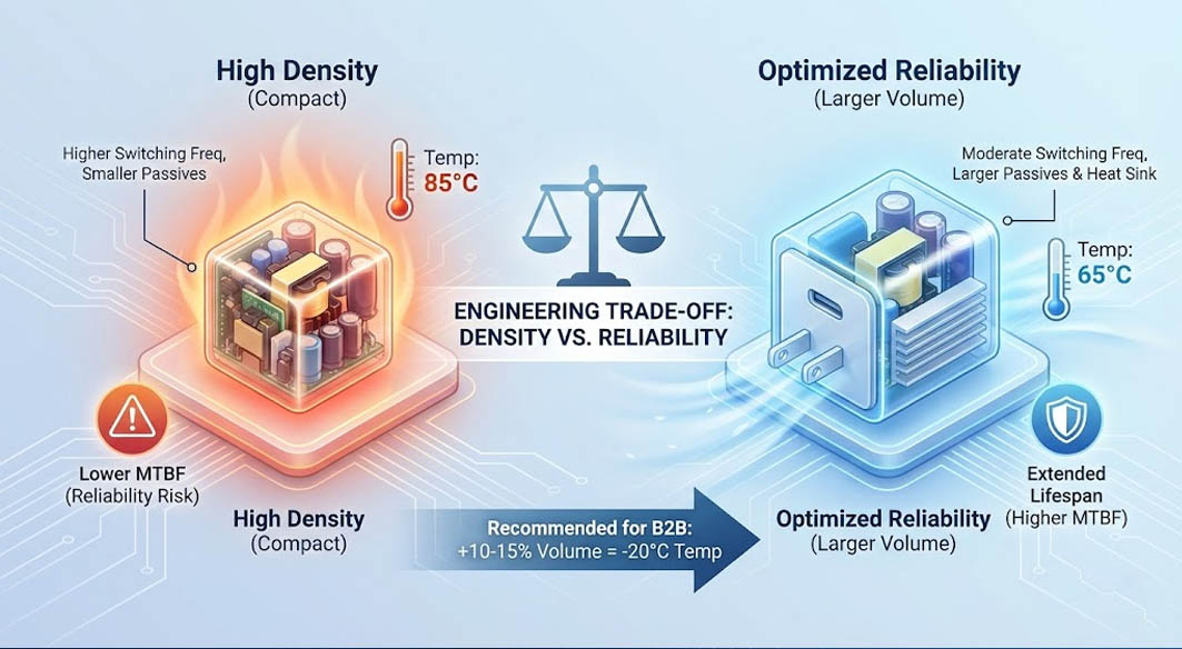
Engineering Trade-off Analysis: Density vs. Reliability
In power electronics, there is no such thing as a perfect design; there are only trade-offs. A critical decision point in pd fast charge architecture is the balance between power density (W/in³) and thermal reliability.
Marketing departments often demand the smallest possible form factor to compete on aesthetics. However, purely from an engineering standpoint, minimizing volume strictly increases thermal impedance. To make a charger smaller, engineers must increase the Switching Frequency Optimization. Higher frequencies allow for smaller passive components (transformers and capacitors), which saves space.
The downside: Switching losses in silicon MOSFETs increase linearly with frequency. This generates more heat in a smaller space. While GaNFast (Gallium Nitride) technology helps mitigate these switching losses, it does not eliminate them. An ultra-compact 65W charger often runs significantly hotter than a slightly larger counterpart. For B2B applications where longevity is paramount, prioritizing extreme density often negatively correlates with MTBF (Mean Time Between Failures). We frequently advise procurement teams to accept a 10-15% volume increase to achieve a 20°C reduction in operating temperature, drastically extending component life.
Technical Architecture and Implementation Strategies
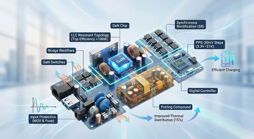
Successful implementation of a high-performance pd 3.0 charger relies on selecting the right topology. For power levels below 75W, the Active Clamp Flyback (ACF) or Quasi-Resonant (QR) Flyback are standard. For power levels above 100W, LLC Resonant topology is preferred due to its soft-switching capabilities, which maximize Efficiency.
Real-world application involves precise layout strategies. For instance, in a specific engineering validation test at Tommox, shifting the primary heat-generating components (bridge rectifiers and GaN switches) to separate PCB zones and utilizing potting compound improved thermal distribution by 15%, preventing hotspot formation that degrades solder joints over time.
Effective design also incorporates:
Synchronous Rectification (SR): Replacing output diodes with MOSFETs to reduce conduction losses on the secondary side.
Programmable Power Supply (PPS): A feature of PD 3.0 that allows the voltage to be adjusted in 20mV steps. This reduces conversion loss inside the phone, shifting the thermal burden away from the battery.
Input Protection: comprehensive MOV and fuse arrangements to handle grid surges, essential for industrial markets with unstable power grids.
Comparing Protocols: PD 3.0 vs. Proprietary Standards
When sourcing charging solutions, it is vital to distinguish between universal standards and proprietary legacy systems. While a generic pd fast charge protocol ensures broad compatibility, understanding the nuance of PPS is critical for modern flagship devices.
Comparison Factors:
Universality: PD 3.0 charger protocols are governed by the USB-IF and work across laptops, tablets, and phones. Proprietary standards (like VOOC or SCP) often require specific cables and chips.
Granularity: PD 3.0 with PPS offers dynamic voltage scaling (3.3V–21V). Legacy protocols often use fixed steps (5V, 9V, 12V), which is less efficient during the Constant Current (CC) charging phase.
Power Ceiling: USB-PD scales up to 240W (PD 3.1), whereas most proprietary phone protocols top out between 60W and 120W and cannot charge laptops.
For B2B distributors, stocking PD-compliant devices minimizes SKU complexity, as a single unit can service a wide array of end-user hardware.
FAQ for Procurement and Product Managers
Q: How does Ripple Control affect the longevity of the connected device?
A: High ripple voltage heats up the receiving device's capacitors and PMIC. A high-quality pd fast charge unit should maintain ripple below 100mVp-p under full load to ensure the safety of the powered equipment.
Q: Is GaN necessary for all PD chargers?
A: Not necessarily. For lower wattages (<30W), silicon-based designs are mature and cost-effective. GaN becomes technically and commercially viable primarily at 45W and above, where the size/efficiency benefits justify the cost premium.
Q: What is the most common failure mode in bulk charger deployments?
A: Electrolytic capacitor dry-out caused by excessive heat is the leading cause of long-term failure. This emphasizes the need for proper Thermal Management in the design phase.
Future Trends in Fast Charging Architectures
The trajectory of pd fast charge technology is moving toward higher voltages to reduce cabling current requirements. The transition from PD 3.0 to PD 3.1 introduces the Extended Power Range (EPR), capable of 28V, 36V, and 48V outputs.
Future designs will focus on:
Digital Control Loops: Moving from analog PWM controllers to MCU-based digital power, allowing for firmware updates and smarter Failure Mode Analysis.
Totem-Pole PFC: Implementing bridgeless Power Factor Correction to push efficiency beyond 96%.
Integration: System-in-Package (SiP) solutions where the gate driver and GaN FET are in a single die to reduce parasitic inductance.
For sourcing managers, the immediate focus should be on ensuring current product lines support PPS, as this is becoming the baseline requirement for fast charging modern smartphones and tablets efficiently.
 Single-Port vs Multi-Port Chargers: Pros and Cons Explained