


Why GaN Chargers Are Smaller and Faster: A Technical Deep Dive
 04 Feb,2026
The transition from Silicon (Si) to Gallium Nitride (GaN) represents the most significant shift in power electronics since the introduction of the MOSFET. For procurement managers and engineers sourcing a charger 65w, understanding the underlying physics is not just academic—it is a critical factor in evaluating product reliability, thermal performance, and longevity.
As an engineer who has spent a decade debugging power topologies, I have seen firsthand how the industry moved from bulky "bricks" to ultra-compact adapters. However, shrinking a device is not merely about using smaller components; it requires a fundamental rethinking of Switching Frequency Optimization and thermal dissipation. This article explores why the modern usb pd charger is superior and how to identify robust designs for B2B applications.
The Physics of GaN: Breaking the Silicon Limit
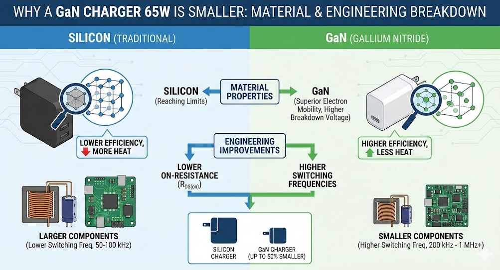
To understand why a GaN-based charger 65w is smaller, we must look at the material properties. Silicon has reached its theoretical limit regarding switching speed and heat dissipation. GaN, a wide-bandgap semiconductor, offers superior electron mobility and a higher breakdown voltage.
In practical engineering terms, this allows for two critical improvements:
Lower On-Resistance (RDS(on)): GaN transistors conduct electricity with significantly less resistance than silicon. Less resistance means less heat is generated during operation, directly improving Efficiency.
Higher Switching Frequencies: Traditional silicon chargers switch at around 50–100 kHz. GaN devices can operate efficiently at 200 kHz to over 1 MHz.
The relationship between frequency and size is governed by the physics of magnetics and capacitance. As the switching frequency increases, the energy required to be stored in the transformer and capacitors per cycle decreases. Consequently, the physical size of the transformer—often the bulkiest component in a usb pd charger—can be reduced by up to 50%.
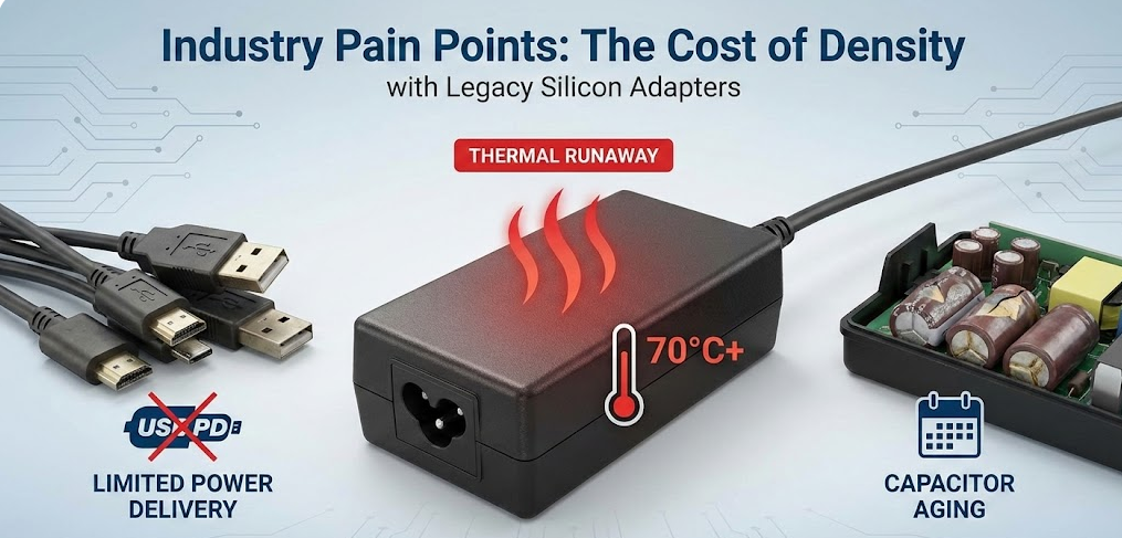
Industry Pain Points: The Cost of Density
Before GaN became commercially viable, increasing power density was a constant battle against thermodynamics. Sourcing managers frequently encountered the following issues with legacy silicon adapters:
Thermal Runaway: To achieve 65W in a smaller form factor using Silicon, engineers had to compromise on thermal headroom. This often led to case temperatures exceeding 70°C, posing safety risks and increasing return rates.
Limited Power Delivery: Older designs struggled to support the full requirements of the usb pd charger standard (specifically PD 3.0 and PPS) without becoming excessively large.
Capacitor Aging: High internal temperatures dry out electrolytic capacitors faster, significantly reducing the Mean Time Between Failures (MTBF).
Engineering Trade-off Analysis: The Frequency Trap
This is the section where I must be brutally honest about the engineering reality. While marketing materials highlight "smaller is better," strictly prioritizing the smallest possible charger 65w often leads to reliability issues.
The Trade-off: Increasing switching frequency reduces the size of magnetics, but it exponentially increases Switching Losses (specifically capacitive turn-on losses) and Electromagnetic Interference (EMI) if not managed correctly.
My Engineering Judgment: A responsible design does not simply chase the highest frequency to achieve the smallest cubic inch volume.
EMI Challenges: High dV/dt (rapid voltage changes) in GaN generates significant EMI noise. If the EMI filter design is weak (to save cost or space), the charger will fail compliance testing or interfere with touchscreens.
Thermal Density: A hyper-compact charger might look sleek, but if it lacks sufficient surface area or thermal potting, it cannot sustain full load for extended periods.
Therefore, the best B2B choice is not the absolute smallest charger, but the one that balances power density with sufficient thermal mass. We prioritize Thermal Management over shaving off the last millimeter of plastic.
Tommox Design Philosophy & Implementation
At Tommox, we approach the charger 65w design with a "Reliability First" methodology. We utilize GaN not just to shrink the device, but to create a cooler, more stable power platform.
Our implementation strategy includes:
Planar Transformers: Instead of wire-wound transformers, we often use PCB-based planar magnetics. This lowers the profile and improves heat dissipation consistency.
Fully Potted Structures: We fill the internal void with high-thermal-conductivity potting compound. This distributes heat evenly from the GaN ICs to the outer casing, preventing hot spots.
Advanced Controller Integration: We utilize controllers that support PPS (Programmable Power Supply) to dynamically adjust voltage and current, reducing conversion losses at the device end.
For distributors looking for reliable stock, our [OEM custom PD charging solutions] offer a balance of cutting-edge density and industrial-grade durability.
Specification & Approach Comparison: Si vs. GaN
When evaluating a charger 65w, the differences between a legacy Silicon design and a modern GaN implementation are measurable.
Power Density:
Silicon: ~10–15 Watts per cubic inch.
GaN: ~20–30+ Watts per cubic inch.
Efficiency (at full load):
Silicon: Typically 87%–89%.
GaN: Typically 93%–95%.
Thermal Delta (Rise above ambient):
Silicon: High rise, requires large heatsinks.
GaN: Lower rise, manageable with potting and layout optimization.
Ripple Control:
Silicon: Often higher due to lower frequency limitations.
GaN: Superior transient response and lower output ripple.
FAQ: Procurement & Technical Inquiries
Q: Does a GaN charger 65w support legacy devices?
A: Yes. A compliant usb pd charger negotiates power. If a legacy device only asks for 5V/2A, the GaN charger will provide exactly that. The high-tech internal topology is transparent to the load.
Q: Why is EMI testing more critical for GaN chargers?
A: The fast switching speeds of GaN create high-frequency noise. You must ensure your supplier provides full EMC reports (FCC/CE) proving they have mitigated this through proper EMI shielding and filter design.
Q: Is the lifespan of GaN proven?
A: Yes. GaN technology has matured significantly. With proper Thermal Management, GaN semiconductors often outlast their silicon counterparts because they undergo less thermal stress during operation.
Q: Can you customize the housing for private labeling?
A: Absolutely. We recommend reviewing our [flexible ODM charger catalog] to see how we can adapt the form factor while maintaining the integrity of the thermal design.
Future Trends & Design Direction
The evolution of the charger 65w is far from over. The next generation of power electronics is moving toward even higher integration.
Totem Pole PFC: We are moving toward bridgeless Totem Pole Power Factor Correction (PFC) topologies, which further eliminate diode drop losses, pushing efficiency toward 97%.
Digital Control: Analog controllers are being replaced by digital cores that allow for firmware updates and adaptive charging algorithms.
GaN-on-Si Integration: Future drivers and GaN FETs will be integrated into single packages, further reducing parasitic inductance and improving Failure Mode Analysis capabilities.
For buyers, staying ahead means partnering with manufacturers who understand that GaN is not just a component change—it is a system-level architectural shift.
 Why USB-C Chargers Are Becoming the New Standard?