


What is GaN Technology? The Future of Fast Charging Explained
 26 Feb,2026
The shift from traditional silicon to Gallium Nitride is fundamentally reshaping power supply design and thermal architecture. When evaluating a commercial-grade GaN fast charger, sourcing teams must move beyond consumer marketing hype and focus strictly on engineering viability. Implementing a robust pd fast charge system requires a deep understanding of the semiconductor’s physical characteristics and its impact on the surrounding circuitry. For B2B applications, long-term reliability and compliance are far more critical than peak theoretical specifications.
Technical Fundamentals Behind a Reliable GaN Fast Charger
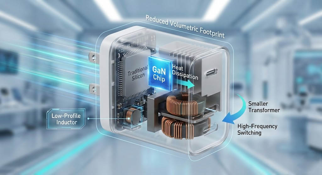
Gallium Nitride is categorized as a Wide Bandgap (WBG) semiconductor material, offering a bandgap of approximately 3.4 eV compared to silicon's 1.1 eV. This physical property allows GaN High Electron Mobility Transistors (HEMTs) to sustain significantly higher electric fields before experiencing avalanche breakdown. Consequently, power electronics engineers can drastically reduce the physical size of the power components while simultaneously maintaining high electrical efficiency.
The primary systemic advantage lies in Switching Frequency Optimization. GaN transistors exhibit virtually zero reverse recovery charge (Qrr) and extremely low gate charge (Qg). This enables high-frequency switching with minimal switching losses (Psw). By pushing the switching frequency from the standard 65 kHz up to 130-300 kHz, designers can specify much smaller magnetic components, such as transformers and EMI chokes, reducing the overall volumetric footprint of the charger.
Industry Pain Points in PD Fast Charge Deployment
Despite the obvious theoretical advantages, the mass production and deployment of high-density adapters introduce severe real-world engineering challenges. Thermal Management remains the most critical hurdle in modern adapter design. Packing 100W or 140W of power into a low-volume, sealed plastic enclosure means that natural convection cooling is non-existent, and conductive heat dissipation paths are severely restricted.
Additionally, operating at these elevated switching frequencies introduces significant EMI (Electromagnetic Interference) and EMC compliance issues. Achieving optimal Ripple Control while passing rigorous global certification standards (such as CISPR 32 or EN 55032) requires highly complex PCB layout techniques. High dv/dt and di/dt transitions inherent to GaN switching create aggressive noise profiles that demand sophisticated shielding and filtering strategies, which can offset the size benefits of the GaN IC.

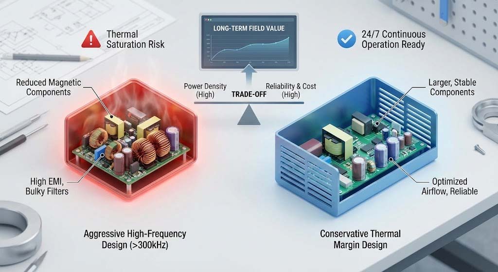
Engineering Trade-off Analysis: The Reality of High Power Density
As an engineering lead, I consistently observe procurement teams being lured by "maximum power in minimum volume" specifications, ignoring the underlying physics. The reality of power electronics is a strict trade-off between power density, thermal reliability, and BOM (Bill of Materials) cost. Pushing a GaN fast charger to extreme switching frequencies (e.g., above 300 kHz) drastically reduces magnetic component size on paper.
However, this aggressive design choice exacerbates high-frequency EMI, requiring bulkier common-mode chokes and Y-capacitors that negate the initial space savings. Furthermore, running components at their absolute thermal limits might pass a short-term datasheet test, but it inevitably leads to premature electrolytic capacitor dry-out and solder joint fatigue in the field. For B2B and enterprise deployments requiring 24/7 continuous operation, a slightly larger enclosure with a conservative thermal margin is structurally superior and far more reliable than an ultra-compact, thermally saturated unit.
Implementation and Design Philosophy in GaN Architectures
Addressing these inherent failure modes requires a systematic approach to the internal physical and thermal architecture. In the Tommox engineering reference case, the design priority fundamentally shifts from absolute volumetric miniaturization to optimized thermal distribution. The implementation utilizes custom thermal potting compounds to create an efficient, low-thermal-resistance bridge from the heat-generating GaN ICs and planar transformers to the outer polycarbonate casing.
This specific layout mitigates localized hot spots on the PCBA (Printed Circuit Board Assembly). Furthermore, the gate drive loops are tightly optimized in the layout to reduce parasitic trace inductance, preventing gate ringing and potentially catastrophic shoot-through events. This factual design methodology explicitly prioritizes Mean Time Between Failures (MTBF) and strict thermal regulation over achieving the smallest possible form factor.
Specification & Approach Comparison
When sourcing managers evaluate legacy Silicon versus modern GaN approaches for high-wattage pd fast charge applications, several engineering parameters must be compared:
Switching Frequency: Traditional Silicon typically operates efficiently at 50-100 kHz. A well-designed GaN fast charger comfortably operates at 130-300 kHz, enabling the use of highly compact planar transformers.
Efficiency Peaks: Silicon-based QR (Quasi-Resonant) flyback topologies peak around 91-93%. Optimized GaN topologies, such as Active Clamp Flyback (ACF) or Asymmetric Half-Bridge (AHB), routinely achieve 94-95.5% efficiency at full load.
Thermal Density Tolerance: GaN systems can theoretically handle higher watts per cubic inch, but they mandate advanced internal heat sinks or potting compounds to prevent enclosure melt or component degradation.
Gate Drive Complexity: Silicon MOSFETs are relatively forgiving regarding gate voltage. GaN HEMTs require highly precise 5V to 6V gate drive regulation; overvoltage can cause immediate gate dielectric breakdown.

FAQ for Sourcing Managers on GaN Fast Charger Projects
How does Programmable Power Supply (PPS) affect GaN thermal profiles? PPS protocols require the pd fast charge controller to adjust voltage and current dynamically in micro-steps based on the receiving device's battery state. This dynamic scaling means the GaN fast charger must maintain high efficiency and stable loop control across a massive output range (e.g., from 3.3V up to 21V), heavily complicating thermal dissipation at high-current, low-voltage states.
What Failure Mode Analysis (FMA) data should we request from OEMs? Always request comprehensive FMA documentation regarding thermal cycling and prolonged maximum load burn-in tests. Pay specific engineering attention to the primary bulk capacitor's predicted lifespan calculations when subjected to internal ambient temperatures exceeding 85°C.
Are planar transformers mandatory for high-density PD adapters? While not strictly mandatory, they are highly recommended for reliability. Traditional wire-wound transformers suffer heavily from proximity and skin effects at high switching frequencies. Planar designs minimize AC winding resistance and offer highly repeatable parasitic parameters, which is crucial for mass-production consistency.
Future Trends & Design Direction
The next technical evolution in GaN fast charger architecture is the move toward extreme integration. The industry is rapidly transitioning to integrated GaN ICs, where the digital controller, analog gate driver, protection circuits, and the primary GaN power FET are co-packaged into a single module. This drastically reduces parasitic inductance on the PCB, simplifying the layout and significantly increasing overall system reliability.
Additionally, the transition from analog control loops to fully digital MCU-based controllers will dominate B2B procurement requirements. Digital control allows for predictive thermal management and intelligent power-sharing algorithms in multi-port designs, adapting in real-time to load transients.
 Deep Dive into the Belkin 112W GaN Charger: Unveiling the Secrets of a Multi-Port Flagship