


How Fast Charging Standards Affect c type phone charger Performance?
 25 Feb,2026
The real-world performance of a phone charger is rarely defined by its raw peak wattage alone. Instead, the underlying fast charging standards dictate the entire hardware architecture, component selection, and ultimate reliability of the unit. For B2B procurement, understanding this protocol-hardware intersection is critical.
When evaluating bulk purchases, focusing purely on power labels often leads to poor field reliability. Modern fast charging protocols require highly dynamic power stages capable of rapid voltage transitions. This article breaks down the engineering reality behind these standards and how they impact product longevity.
Technical Fundamentals Behind a c type phone charger
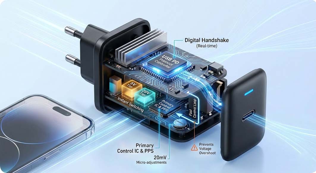
At the core of any modern charging adapter is the communication protocol, primarily USB Power Delivery (PD). This standard requires a constant digital handshake between the power source and the receiving device. The protocol dictates the output voltage and current in real-time.
To support these dynamic requests, the power stage must utilize advanced control ICs. When a device requests a shift from 5V to 20V, the primary side controller must adjust its duty cycle instantly. This requires rigorous Switching Frequency Optimization to maintain efficiency across different voltage tiers.
Furthermore, features like Programmable Power Supply (PPS) demand micro-adjustments of 20mV steps. This continuous voltage scaling places immense stress on the feedback loop and secondary synchronous rectification. If the control loop response is too slow, it results in voltage overshoot, triggering device protection mechanisms.
Industry Pain Points in a multiport charger
Transitioning from a single output to a multiport charger scales the engineering complexity non-linearly. The primary challenge is no longer just AC-DC conversion, but intelligent DC-DC power allocation. Microcontroller units (MCUs) must constantly renegotiate power limits based on plug-in/plug-out events.
This constant renegotiation introduces several severe industry pain points:
Thermal Bottlenecks: Multiple DC-DC buck converters operating in close proximity create severe localized hotspots on the PCB.
Protocol Conflicts: Poorly coded MCU logic can cause constant connection dropping when devices with differing protocol requirements are plugged in simultaneously.
Poor Ripple Control: Under heavy load, especially when multiple ports approach maximum capacity, output ripple often exceeds standard limits, accelerating battery degradation.
Engineering Trade-off Analysis: Spec vs. Reality
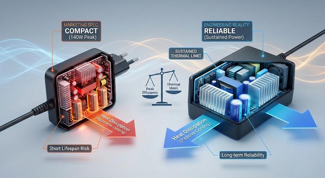
In B2B applications, chasing the absolute highest power density often leads to compromised long-term reliability. There is a fundamental engineering conflict between marketing specifications and the physics of Thermal Management. A highly compact 140W adapter might look appealing on a spec sheet, but it often relies on aggressive thermal derating logic.
When subjected to a continuous 72-hour burn-in test at full load, these ultra-compact designs frequently fail or severely throttle output. To shrink the form factor, engineers must use smaller bulk capacitors and reduce heat sink mass. This increases the internal operating temperature, drastically reducing the lifespan of electrolytic capacitors.
For commercial applications like hospitality or enterprise IT deployments, a physically larger enclosure is often the superior engineering choice. A larger volume allows for passive heat dissipation without relying on aggressive NTC (Negative Temperature Coefficient) throttling. True engineering requires balancing:
Peak Efficiency vs. Thermal Mass: High efficiency (e.g., 94%) minimizes heat, but adequate copper mass is still required for worst-case scenarios.
Component Lifespan vs. BOM Cost: High-temperature rated capacitors (105°C) increase costs but are mandatory for tight enclosures.
Marketing Power vs. Sustained Power: B2B buyers should request "sustained thermal limit" data rather than "peak burst power."
Protocol Implementation & Design Approach
Designing a power stage that complies with stringent PD 3.1 and PPS requirements necessitates specific architectural choices. The primary constraint is managing the leakage inductance and switching losses during high-voltage output scenarios. Standard flyback topologies struggle with efficiency when outputting 28V or higher.
To address the thermal concentration during sustained 100W+ output phases, one engineering reference case evaluated by Tommox involved implementing an asymmetric half-bridge flyback (AHB) topology paired with planar transformers. This specific design choice physically distributes the magnetic core losses across a wider PCB footprint.
Consequently, this distributed thermal profile prevents localized overheating near the critical primary switching nodes. However, the trade-off involves a more complex PCB layout and stricter tolerance requirements for the planar magnetic layers. It demonstrates that handling high-tier charging standards relies heavily on physical layout physics.
Specification & Approach Comparison for a c type phone charger
Different charging protocols require vastly different hardware implementations. Sourcing managers must align the hardware capabilities with their specific market requirements.
Standard PD 3.0 (Fixed Voltages): Requires standard synchronous rectification. Cost-effective, highly reliable, and sufficient for basic laptop and tablet deployments.
PD 3.0 with PPS: Requires a secondary-side MCU capable of 20mV/50mA micro-adjustments. Higher BOM cost, necessitates tighter Ripple Control, but critical for modern smartphone fast charging.
PD 3.1 Extended Power Range (EPR): Operates up to 28V/36V/48V. Requires highly specialized GaN power ICs and components rated for significantly higher voltage stress.
For enterprise-level procurement, reviewing [Commercial Grade Power Adapters] requires analyzing which of these protocols is actually necessary for the end-user deployment.
FAQ for B2B Sourcing Managers
Q: How does the PPS standard impact the failure rate of a phone charger? PPS requires continuous voltage adjustment, which increases the operational stress on the optocoupler and feedback loop. If low-tier components are used, Failure Mode Analysis frequently points to feedback loop degradation over time.
Q: Why does a multiport charger reset when a new device is plugged in? This is an intentional protection mechanism. The MCU must pause power delivery to safely renegotiate the power allocation map based on the newly available power budget and the requested protocols of both devices.
Q: Are GaN components mandatory for PD 3.1 standards? While not strictly mandatory by the specification, GaN devices are practically required to meet the efficiency and form-factor expectations of high-voltage (28V+) EPR outputs without catastrophic thermal runaway.
Future Trends & Design Direction
The future of the c type phone charger lies in deeper silicon integration. We are moving away from discrete GaN transistors toward fully integrated GaN ICs (like GaNFast solutions) that combine the controller, driver, and switch in a single package.
Furthermore, digital control loops will replace traditional analog feedback systems. This will allow firmware-level optimization of the switching frequency based on the specific device connected, maximizing efficiency across all load profiles. B2B buyers should anticipate a shift towards highly programmable, firmware-updatable power architectures.
 What is GaN Technology? The Future of Fast Charging Explained