


Fast Charger vs Standard Charger: What’s the Real Difference?
 10 Feb,2026
In the current landscape of consumer electronics power delivery, the distinction between a legacy adapter and a modern GaN fast charger extends far beyond the wattage rating printed on the label. For B2B buyers and product managers, understanding the underlying circuit topology and material science is critical for selecting reliable suppliers.
While standard silicon-based chargers rely on lower-frequency switching and bulky magnetics, the GaN fast charger represents a fundamental shift in power density and efficiency. This article dissects the engineering trade-offs, thermal challenges, and protocol implementations that define high-performance power supply units (PSUs).
Technical Fundamentals of the GaN Fast Charger Architecture
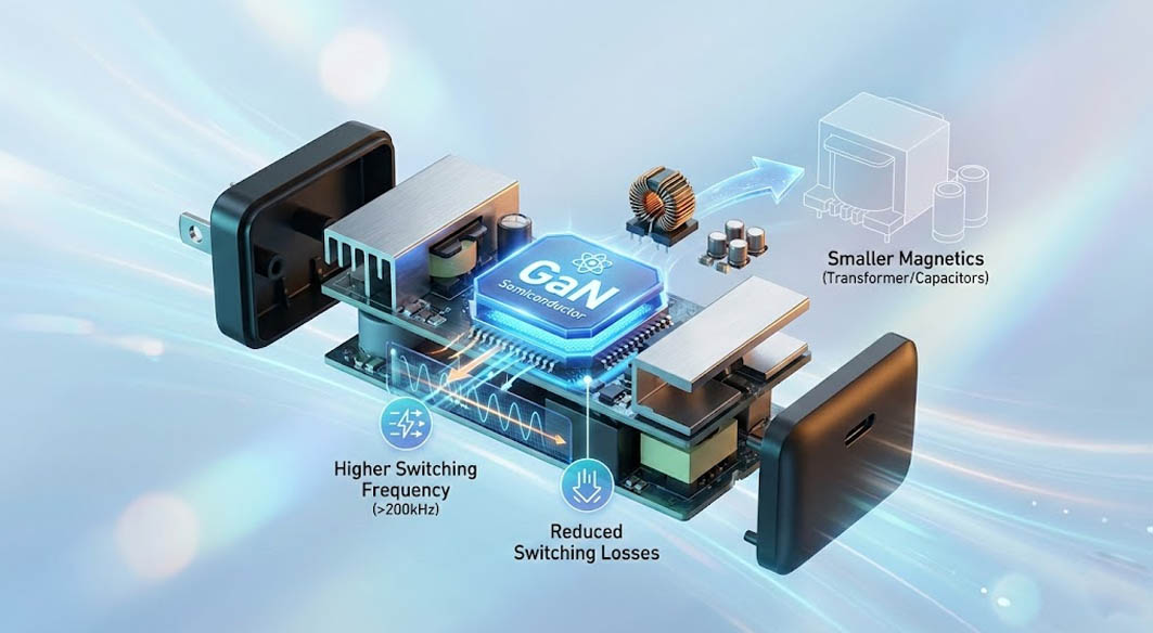
The core differentiator lies in the semiconductor material. Standard chargers utilize Silicon (Si) MOSFETs, which have a theoretical limit regarding electron mobility and breakdown voltage. In contrast, Gallium Nitride (GaN) is a wide-bandgap semiconductor.
This material property allows the GaN fast charger to operate at significantly higher switching frequencies.
Switching Frequency Optimization: While standard Si chargers typically operate between 50kHz and 100kHz, GaN topologies often push beyond 200kHz or even 500kHz.
Magnetics Reduction: Higher frequencies allow for a drastic reduction in the size of transformers and capacitors, which are usually the bulkiest components on the PCBA.
Reduced Switching Losses: GaN transistors have lower Gate Charge and On-Resistance , resulting in minimal energy loss during the transition between on and off states.
Industry Pain Points in Legacy Power Adapters
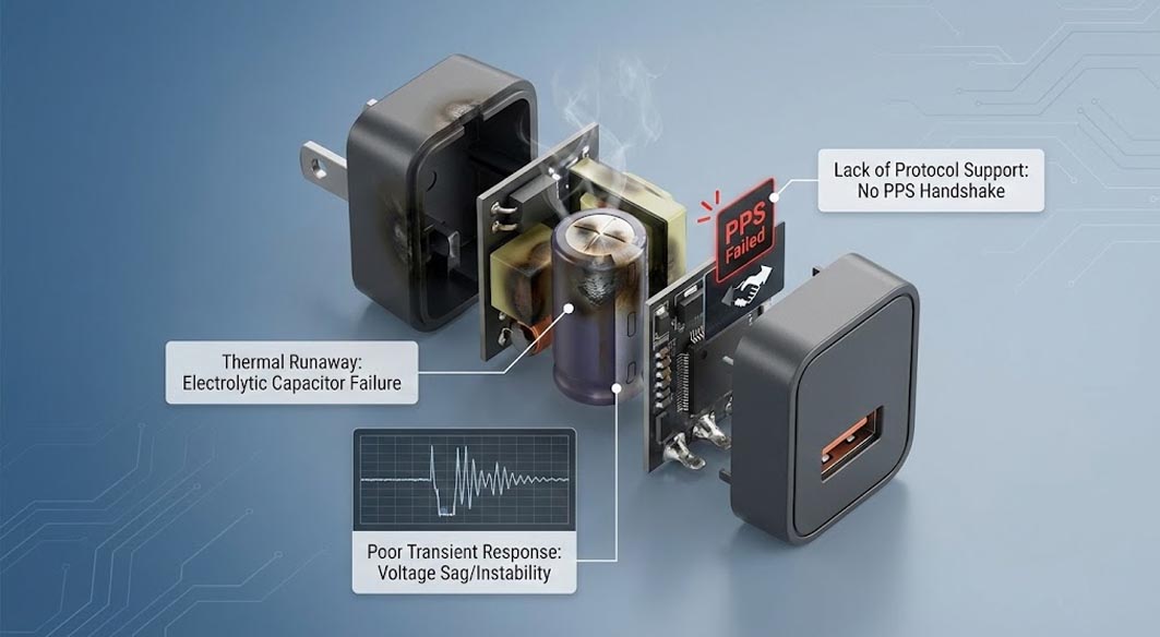
Sourcing managers often encounter high return rates with standard chargers due to inherent design limitations. The reliance on older topology, such as basic hard-switching Flyback converters, creates specific Failure Mode Analysis scenarios.
Thermal Runaway: Due to lower efficiency (often <85%), standard chargers generate excess waste heat. In enclosed plastic housings, this leads to component degradation over time, particularly for electrolytic capacitors.
Poor Transient Response: Legacy adapters often struggle to adapt quickly to the dynamic load changes of modern smartphones or laptops, leading to voltage sags.
Lack of Protocol Support: Most standard units lack advanced handshaking capabilities like PPS (Programmable Power Supply), forcing devices to charge at fixed, inefficient voltage levels.
Engineering Trade-off Analysis: Density vs. Thermal Headroom
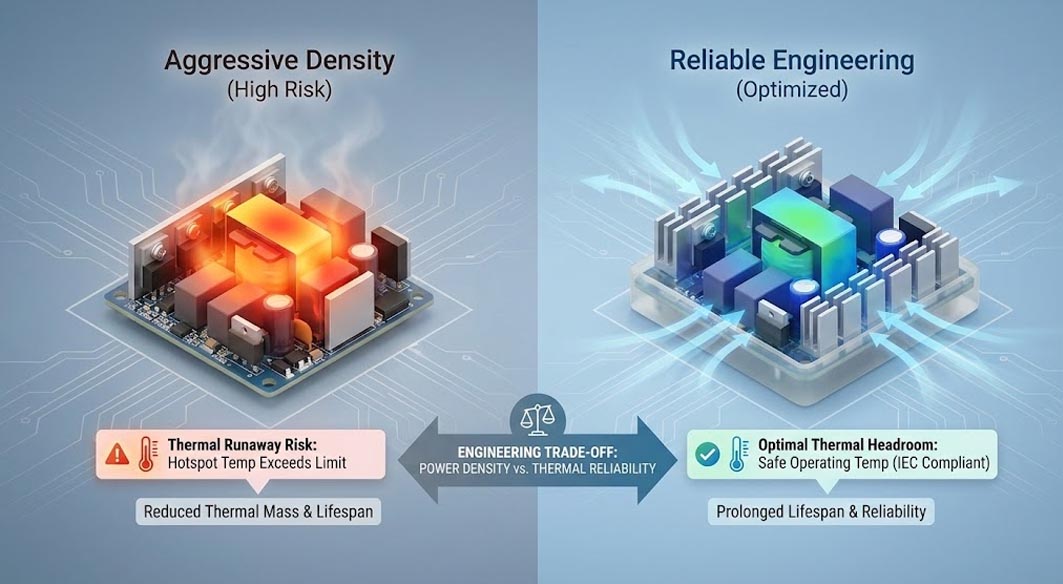
A critical aspect of power supply design that is often overlooked in spec sheets is the aggressive trade-off between power density (W/in³) and thermal reliability. There is a misconception that "smaller is always better." From an engineering standpoint, this is not always accurate for long-term reliability.
Pushing a GaN fast charger to the absolute minimum physical size requires clustering heat-generating components (MOSFETs, Transformers, Rectifiers) closer together. While this achieves a marketing claim of "world's smallest," it drastically reduces thermal mass. Without adequate spacing or heatsinking, the hotspot temperature can exceed safe operating limits under continuous load.
Reliable engineering involves a deliberate decision to sacrifice a percentage of volume reduction to gain thermal headroom. A slightly larger PCBA allows for better airflow or the inclusion of potting compounds, ensuring that the device remains cool enough to touch (adhering to IEC 62368-1 standards) and prolonging the lifespan of the control ICs.
Implementing Advanced Protocols and Circuit Design
To mitigate the risks associated with high-frequency switching, such as Electromagnetic Interference (EMI) and output noise, sophisticated design strategies must be employed.
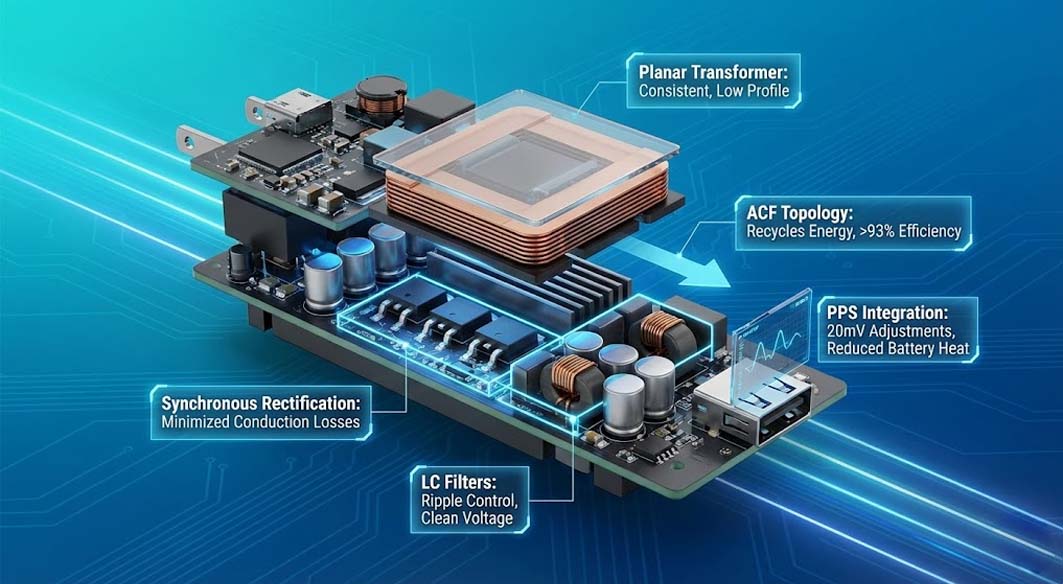
In a specific Tommox engineering reference case regarding 100W PD modules, the design team opted to implement a specialized synchronous rectification scheme rather than a standard diode setup. This choice, while increasing the bill of materials (BOM) cost, was necessary to minimize conduction losses at high currents. Furthermore, the inclusion of additional LC filters was prioritized to manage Ripple Control, ensuring that the voltage delivery remained clean enough for sensitive laptop motherboards, even though it slightly increased the overall footprint of the internal layout.
Key engineering implementations in modern GaN fast charger designs include:
Active Clamp Flyback (ACF) Topology: Recycles leakage energy that would otherwise be dissipated as heat, boosting efficiency to over 93%.
Planar Transformers: Replaces wire-wound bobbins with PCB-stacked windings for consistent consistency and lower profile.
PPS Integration: Allows the sink device (phone/laptop) to request voltage adjustments in 20mV steps, reducing conversion heat inside the battery.
Specification & Approach Comparison
For procurement teams evaluating OEM proposals, the following comparison highlights the structural differences between standard and GaN-based solutions.
Topology:
Standard: Quasi-Resonant (QR) Flyback or Hard Switching.
GaN Fast Charger: Active Clamp Flyback (ACF) or LLC Resonant Converter.
Efficiency:
Standard: Typically 80% – 85%.
GaN Fast Charger: Typically 92% – 95% (Crucial for Thermal Management).
Power Density:
Standard: 0.5 – 0.8 W/cm³.
GaN Fast Charger: > 1.2 W/cm³.
EMI Handling:
Standard: Easier to filter due to low frequency.
GaN Fast Charger: Requires complex shielding and differential mode filtering due to high dV/dt.
If you are looking to upgrade your product line, consider reviewing our guide on [OEM power supply customization constraints and possibilities].
FAQ for Sourcing Managers and Technical Leads
Q: Does a GaN fast charger inherently have a higher failure rate due to heat density?
A: Not if designed correctly. While density is higher, the efficiency gain means less heat is generated per watt. However, poor Thermal Management in ultra-miniature designs can lead to early failure.
Q: Why is Ripple Control important for B2B applications?
A: High ripple voltage can interfere with the touch sensitivity of screens and degrade the battery life of the connected device. B2B clients require strict ripple specs (usually <100mVp-p).
Q: Is PPS mandatory for all fast chargers?
A: While not mandatory, PPS is essential for efficiently charging modern Android flagships (Samsung, etc.). Without PPS, these devices will revert to slower charging speeds to protect their batteries.
Future Trends in GaN Fast Charger Development
The evolution of the GaN fast charger is moving toward higher integration and Totem-Pole PFC architectures.
Integrated GaN ICs: Manufacturers are moving away from discrete components to "GaNFast" style chips that integrate the driver, FET, and protection logic into a single package, reducing parasitic inductance.
Digital Control: The shift from analog to digital controllers allows for adaptive switching frequencies based on real-time load analysis.
Beyond 240W: With the USB PD 3.1 standard, we will see GaN designs scaling up to 240W, challenging the dominance of traditional heavy brick adapters for gaming laptops.
 How Fast Charging Standards Affect c type phone charger Performance?