



Inside Aohai’s Compact 60W GaN Dynamic Fast Charger: Design, Performance and Component Teardown
 20 Jul,2026
A Compact 60W GaN Charger Designed for Modern Devices
As fast-charging technology continues to evolve, consumers increasingly expect chargers to deliver higher power in a smaller and lighter form factor. Smartphones, tablets, handheld gaming devices and lightweight laptops now commonly support USB-C Power Delivery, creating strong demand for compact chargers capable of serving multiple types of devices.
Aohai’s 60W GaN dynamic fast charger is designed around this trend. It combines a maximum output of 60W with a compact square housing, a single USB-C port and broad compatibility with mainstream fast-charging protocols.
The charger supports fixed PD output up to 20V/3A and programmable PPS output up to 21V/3A. It also supports AVS voltage regulation, making it suitable for newer USB Power Delivery applications that require more flexible voltage control.
In addition to its charging performance, the product features an average conversion efficiency that meets DOE Level VI and CoC Tier 2 energy-efficiency requirements. At the 20V output level, its efficiency can reach approximately 87.5%.
The rated mean time between failures, or MTBF, is up to 30,000 hours. Multiple protection mechanisms, including overcurrent protection, overvoltage protection and short-circuit protection, are integrated to improve operational reliability.
This article takes a closer look at the charger’s exterior design, charging protocols, physical dimensions, circuit architecture and key internal components.
Minimalist Exterior Design
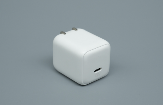
The charger adopts a clean white square design with rounded edges. Its enclosure is manufactured from flame-retardant polycarbonate material, helping the product meet the safety and durability requirements expected from a high-power USB-C charger.
A matte surface treatment gives the housing a smooth and refined texture. Compared with glossy plastic, the matte finish is less likely to collect visible fingerprints and scratches during everyday use.
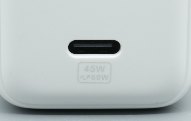
The front of the charger contains one USB-C output port. A “45W–60W” dynamic power marking is printed below the port, highlighting the charger’s variable power-output capability.
The remaining sides contain no large logos or decorative graphics, maintaining a simple and professional appearance. This type of minimalist housing can also be adapted for OEM and ODM charger projects that require customized branding, printing or laser engraving.
The AC pins feature a foldable structure, making the charger easier to store in a bag or travel case. Foldable pins also help reduce accidental scratching of nearby devices during transportation.
This version uses the latest Chinese-standard AC pin design.
Electrical Specifications
The laser-engraved product information includes the following specifications:
Product name: GaN Dynamic Fast Charger
Model: A1266-200300C-CN1
Input: 100–240V AC, 50/60Hz, 1.5A Max
USB-C fixed output: 5V/3A, 9V/3A, 12V/3A, 15V/3A and 20V/3A
AVS output: 9–15V/3A and 15–20V/2.25A, with 3A dynamic power support
PPS output: 5–21V/3A
Maximum output power: 60W
The 100–240V universal input allows the basic power platform to be used across many global markets, provided that the AC plug design and relevant regional certifications are adjusted accordingly.
Fast-Charging Protocol Compatibility
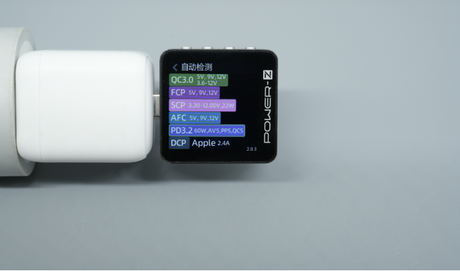
Protocol testing was performed using a POWER-Z KM003C USB power tester. The results showed support for a broad range of charging standards, including:
USB Power Delivery 3.2
PPS
AVS
Qualcomm QC 3.0
Qualcomm QC 5
Huawei FCP
Huawei SCP
Samsung AFC
Apple 2.4A
USB BC1.2 DCP
This broad protocol coverage allows the charger to provide fast charging for many smartphones, tablets, portable electronics and USB-C laptops.
The charger’s PDO information includes five fixed voltage levels:
5V/3A
9V/3A
12V/3A
15V/3A
20V/3A
It also provides programmable voltage ranges for AVS and PPS applications. Depending on the connected device and charging protocol, the charger can adjust the output voltage rather than being limited to fixed voltage steps.
During an actual iPhone charging test, the measured output was approximately 14.24V at 2.02A, corresponding to around 28.91W. The result confirmed that the charger successfully established USB PD fast charging with the device.
Actual charging power will vary according to the device model, battery level, temperature, charging cable and the power-management strategy of the connected device.
Dimensions and Weight
Despite its 60W maximum output, the charger remains compact and lightweight.
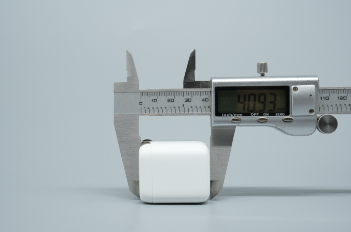
Its measured dimensions are approximately:
Length: 40.93mm
Width: 34.41mm
PCBA height: 35.94mm
PCBA width: 28.74mm
Net weight: 65g
The charger can easily fit into the palm of an adult hand. Compared with some lower-power dynamic chargers, the Aohai 60W charger demonstrates strong volume control and power density.
Its compact size is made possible by a combination of GaN power technology, highly integrated control chips, optimized magnetic components and dense PCB layout.
Internal Construction and Thermal Management
After opening the enclosure, the internal PCBA module can be seen surrounded by a large amount of grey thermal potting compound.
The thermal compound serves several purposes. It transfers heat from the internal components to the outer housing, reduces mechanical movement, provides additional structural support and helps protect components during transportation or accidental impact.
Thermal pads and insulation sheets are also used around the PCB assembly. These materials support heat dissipation while maintaining the electrical isolation required between high-voltage and low-voltage sections.
After the thermal material is removed, the main transformer, high-voltage capacitors, output capacitor and other components become visible.
The component side of the PCBA contains the EMI filtering circuit, high-voltage electrolytic capacitors, transformer, output filtering capacitor, synchronous rectification components and USB-C receptacle.
The rear side contains the input fuse, bridge rectifier, integrated GaN power controller, optocoupler, synchronous rectifier MOSFET, charging protocol controller and VBUS switch MOSFET.
The overall power supply uses a QR flyback architecture. Quasi-resonant flyback designs are widely used in compact USB-C PD chargers because they can balance conversion efficiency, circuit complexity, electromagnetic compatibility and production cost.
Input Protection and EMI Filtering
A surface-mounted fuse is installed at the AC input. The fuse provides basic protection by interrupting the circuit if an abnormal current condition occurs.
A green NTC thermistor is positioned nearby to suppress the inrush current generated when the charger is first connected to AC power.
The input stage also contains two filtering inductors with heat-shrink insulation. These components help reduce conducted electromagnetic interference and prevent high-frequency switching noise from returning to the AC power line.
Two high-voltage aluminum electrolytic capacitors from BERYL are used for primary-side energy storage and filtering. Each capacitor is rated at 400V and 33μF.
The input bridge rectifier is a PANJIT RMSB4M. It is rated at 1000V and 4A and uses an MSBL package. The bridge rectifier converts the incoming AC voltage into high-voltage DC for the primary switching circuit.
A Koshin capacitor rated at 100V and 4.7μF supplies the primary control circuit.
Integrated GaN Primary Power Controller
The primary controller is the Injoinic IP2075_38D, a highly integrated multimode AC/DC flyback controller with a built-in GaN FET.
Integrating the GaN switching device and control functions into one package reduces the required PCB area and simplifies the surrounding circuit. This is particularly important in compact high-power-density charger designs.
The IP2075_38D supports adaptive multimode control and secondary-side regulation. It is designed for applications requiring high power density and accurate output-voltage and output-current control.
The chip includes a high-voltage startup circuit, eliminating the need for a conventional startup resistor. This helps reduce standby power consumption.
When AC input power is removed, the high-voltage pin can also assist with X-capacitor discharge. The design helps lower discharge-related losses and supports low standby power.
Frequency foldback and valley-switching technologies are used to reduce switching losses. Frequency modulation also helps improve EMI performance by spreading switching noise across a wider frequency range.
Under light-load or no-load conditions, the chip enters burst mode. Its operating current in this mode can be as low as approximately 160μA, helping the complete charger meet demanding energy-efficiency standards such as DOE Level VI and CoC requirements.
The controller also supports multiple protection and configuration functions, including:
Output overvoltage protection
Output undervoltage protection
Brown-in and brown-out protection
Overtemperature protection
Compensated overpower protection
Configurable maximum switching frequency
The IP2075_38D uses a DFN18L 6mm × 8mm package.
Transformer and Isolation Components
The high-frequency transformer is marked ATQ17-A1266. It transfers energy from the high-voltage primary side to the low-voltage secondary side while maintaining electrical isolation.
A blue safety Y capacitor marked B471K is installed between the primary and secondary sections to reduce common-mode interference.
An optocoupler marked C604 provides isolated feedback communication between the secondary output circuit and the primary control circuit.
These components are essential for maintaining stable regulation, isolation safety and acceptable electromagnetic compatibility.
Secondary-Side Synchronous Rectification
The charger uses an Injoinic IP2028 synchronous rectification controller.
The IP2028 supports a wide output-voltage range from 3.3V to 28V and can remain compatible with output conditions down to 0V. This makes it suitable for USB PD and PPS chargers where the output voltage changes according to the connected device.
Its integrated voltage-regulation circuit allows the controller to operate without an additional auxiliary winding. It supports both high-side and low-side rectification and is compatible with CCM, DCM, quasi-resonant and ZVS operating modes.
The chip uses Vds volt-second detection to help prevent false MOSFET turn-on caused by ringing under DCM, QR or ZVS conditions.
A pre-turn-off threshold of approximately −30mV and a switching delay of around 30ns allow the MOSFET to turn off quickly and accurately.
Its standby current is approximately 30μA. The device uses a compact SOT23-6 package and requires only a small number of external components.
The synchronous rectifier MOSFET is a CR Micro CRSM049N10L4Z. It is rated at 100V, has an on-resistance of approximately 4mΩ and uses a DFN 5mm × 6mm package.
By replacing a conventional secondary rectifier diode with an actively controlled MOSFET, the synchronous rectification circuit reduces conduction losses and improves overall efficiency.
USB-C Protocol and Output Control
The USB-C output is controlled by the Injoinic IP2723T fast-charging protocol IC.
The IP2723T has passed USB-IF PD 3.0 PPS certification under TID 3135. It is designed for USB output applications and integrates support for multiple fast-charging standards.
Supported functions include USB Type-C DFP, PD 2.0, PD 3.0, PPS, QC 2.0, QC 3.0, QC 4, QC 4+, Huawei FCP, Huawei SCP, Samsung AFC, MediaTek PE, Apple 2.4A and BC1.2.
Its high level of integration allows the complete USB-C output and protocol circuit to be implemented with relatively few external components. This helps reduce PCB space, simplify the BOM and control manufacturing cost.
The output VBUS switch uses a Vergiga Semiconductor VS3618BE N-channel MOSFET. It is rated at 30V and has an on-resistance of approximately 5.2mΩ. The device uses a PDFN3333 package.
A BERYL 25V 680μF electrolytic capacitor is used for secondary-side output filtering. This capacitor helps reduce output ripple and supports stable transient performance when the connected device changes its power demand.
Final Assessment
The Aohai 60W GaN dynamic fast charger demonstrates how a high-power USB-C charger can be integrated into a compact 65g enclosure.
Its main advantages include 60W maximum output, PD 3.2 compatibility, PPS and AVS voltage regulation, broad legacy protocol support, foldable AC pins and a high-density internal layout.
The power architecture combines an Injoinic integrated GaN primary controller, a dedicated synchronous rectification controller and a highly integrated USB-C protocol IC. Together with quality capacitors, low-resistance MOSFETs, thermal potting material and multiple protection mechanisms, the design provides a balanced solution for efficiency, size and reliability.
For charger brands, distributors and OEM customers, this type of platform is suitable for developing compact USB-C power adapters for smartphones, tablets, portable devices and lightweight laptops.
As USB PD, PPS and AVS adoption continues to expand, compact 60W GaN chargers with flexible output capabilities are likely to become an increasingly important category in the global charging accessories market.
 Lenovo 68W GaN Charger Teardown: Compact Design, GaN Technology and Full Component Analysis