



Lenovo 68W GaN Charger Teardown: Compact Design, GaN Technology and Full Component Analysis
 28 Jul,2026
Lenovo has continued to expand beyond laptops, tablets and smartphones by developing a more complete ecosystem of charging accessories. Its current product portfolio includes USB-C chargers, power strips, power banks, charging cables and other power-related accessories designed for both mobile devices and notebook computers.
This article examines the internal design of Lenovo’s 68W single-port GaN charger. With a compact black enclosure, one USB-C output and support for mainstream fast-charging protocols, the charger is designed to power Lenovo laptops, tablets and smartphones, as well as many other USB-C devices.
More importantly, the teardown reveals a highly integrated power architecture built around components from Injoinic, Innoscience, Pingwei and AiSHi. Let us take a closer look at its exterior design, charging specifications, protocol support, thermal management and internal component selection.
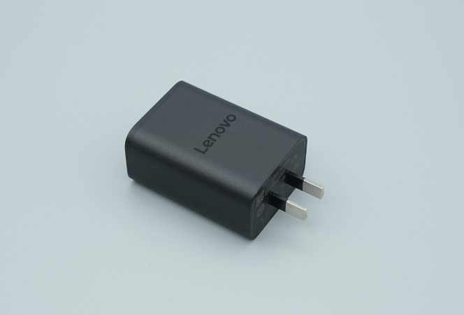
Lenovo 68W GaN Charger Overview
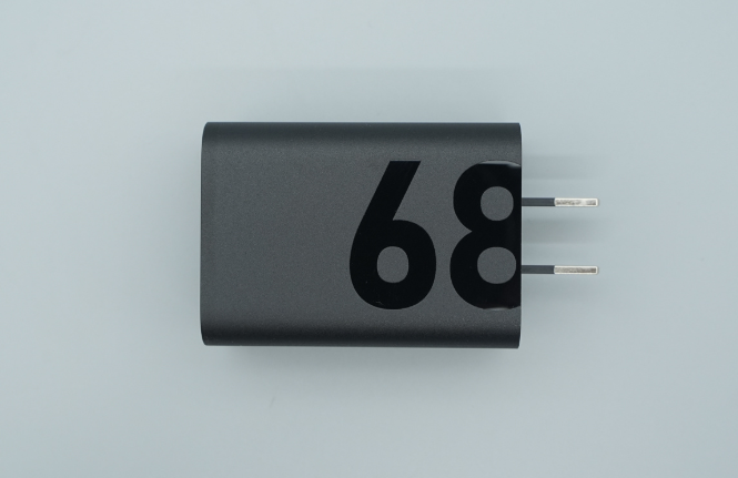
The Lenovo 68W charger uses a simple rectangular design with a matte black finish. A Lenovo logo is printed on one side of the housing, while a large “68” marking occupies most of the opposite side.
Its straight body lines and slightly beveled edges give the charger a clean, modern appearance while also improving handling comfort. Unlike chargers with foldable AC pins, this model uses a fixed two-pin Chinese-standard plug.
The output side is equipped with a single centrally positioned USB-C port. The red internal plastic tongue provides a visual contrast against the black enclosure and makes the connector easier to identify.
Overall, the exterior follows Lenovo’s familiar industrial design language: simple, functional and easy to recognize.
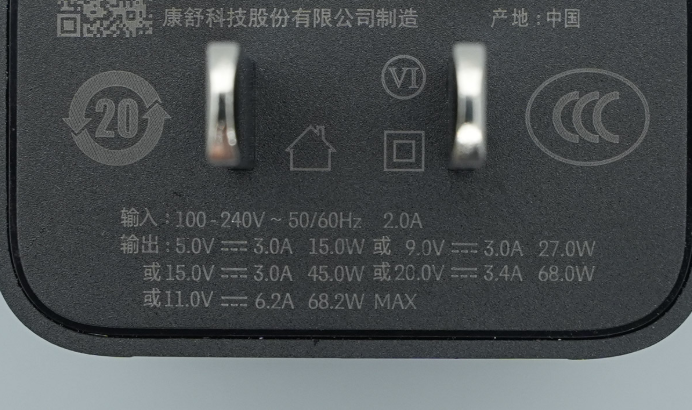
Key Specifications
The product information printed on the charger provides the following specifications:
Model: MC-688
Input: 100–240V AC, 50/60Hz, 2.0A
USB-C output: 5V/3A, 9V/3A, 15V/3A, 20V/3.4A and 11V/6.2A
Maximum output power: 68.2W
Manufacturer: AcBel Polytech Inc.
Certification: CCC and other applicable markings
USB-C ports: One
The charger supports universal 100–240V AC input, allowing the same power platform to operate across different mains voltage environments when used with the appropriate plug configuration.
Its highest standard USB Power Delivery output is 20V/3.4A, equivalent to 68W. This makes it suitable for lightweight laptops, tablets, handheld gaming devices and high-performance smartphones that support USB-C Power Delivery.
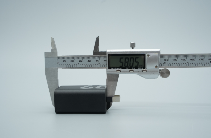
Size and Weight
The measured dimensions of the Lenovo 68W charger are approximately:
Length: 58.05mm
Width: 42.14mm
Thickness: 28.13mm
Weight: 81.7g
For a charger capable of delivering up to 68W, the enclosure is relatively compact. When placed next to Apple’s 70W USB-C power adapter, the Lenovo charger shows a noticeable advantage in overall volume.
The smaller size is largely made possible by the use of a gallium nitride power transistor, a compact PCB layout and densely arranged internal components.
USB-C Fast-Charging Protocol Support
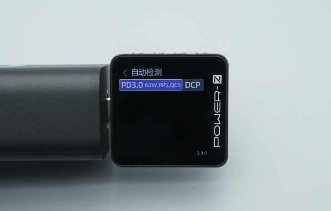
Protocol testing with a POWER-Z KM003C analyzer shows that the USB-C port supports several common charging protocols, including:
USB Power Delivery 3.0
Programmable Power Supply
Qualcomm Quick Charge 5
DCP charging
The USB Power Delivery PDO information includes four fixed voltage profiles:
5V/3A
9V/3A
15V/3A
20V/3.4A
The charger also provides two PPS voltage ranges:
5–11V at up to 5A
5–20V at up to 3.4A
PPS support is particularly useful for modern smartphones that dynamically adjust charging voltage and current. Instead of relying only on fixed voltage levels, the charger can communicate with compatible devices and provide a more precise output.
This can help improve charging efficiency, reduce unnecessary voltage conversion inside the device and control heat during high-power charging.
The 20V/3.4A output also enables the charger to deliver close to its full rated power to compatible notebooks and other USB-C devices.
Opening the Charger
The teardown begins by opening the housing from the AC input side. Once the rear cover is removed, a large amount of white thermal compound can be seen inside the enclosure.
The fixed AC pins are connected to the PCB assembly through insulated wires. The internal PCBA module is also secured with adhesive, helping prevent movement during transportation and everyday use.
After the complete module is removed from the outer shell, both sides of the PCB can be seen covered with white adhesive and thermal material. Major components, including the transformer, inductors and capacitors, are surrounded by compound.
This design serves several purposes:
It secures components against vibration and mechanical stress
It improves heat transfer from internal components to the enclosure
It increases insulation between high-voltage components
It reduces the possibility of component movement or audible noise
A black insulating sheet and a large metal heat-spreading plate are installed on the back of the PCBA. Thermal compound is applied between these layers to transfer heat away from the PCB.
Internal PCBA Dimensions
The internal PCB assembly measures approximately:
Length: 54.55mm
Width: 38.01mm
Thickness: 22.41mm
The internal module occupies most of the available enclosure space. This indicates that Lenovo and AcBel used a highly space-efficient mechanical design rather than leaving large unused areas inside the charger.
After removing the thermal plate, insulation sheet and adhesive, the component arrangement becomes visible. The primary and secondary sides are clearly separated, while surface-mounted components are placed in a compact but orderly layout.
Input Protection and EMI Filtering
The AC input stage includes several protection and filtering components.
A time-delay fuse provides basic protection against excessive current and serious internal faults. A common-mode choke helps reduce conducted electromagnetic interference from the switching power supply.
The charger also uses a green NTC thermistor marked 5S030M. The thermistor limits the initial inrush current that occurs when the charger is connected to the AC mains and the high-voltage capacitors begin charging.
A differential-mode inductor is also installed and covered with black heat-shrink tubing for insulation.
Together, these components form the input protection and electromagnetic interference filtering stage. This stage is important for maintaining stable operation and meeting relevant electromagnetic compatibility requirements.
Rectification and High-Voltage Filtering
Three RS4MBF surface-mounted diodes are visible on the PCB and are used as part of the bridge rectification circuit.
After the AC input is rectified, the resulting high-voltage DC is filtered by three AiSHi aluminum electrolytic capacitors. Each capacitor is rated at:
400V
22μF
The use of three capacitors allows the available capacitance to be distributed across a compact area of the PCB.
Another AiSHi aluminum electrolytic capacitor, rated at 100V and 4.7μF, provides filtering and power supply support for the primary controller.
AiSHi is a well-established capacitor manufacturer frequently used in power adapters and consumer electronics. Its presence contributes to the charger’s overall component quality.
Injoinic IP2006H Primary Controller
The primary-side controller is the Injoinic IP2006H, a high-performance multi-mode flyback controller designed for compact power adapters.
The IP2006H supports frequency foldback and valley switching. These functions help improve power conversion efficiency by adjusting the switching behavior according to operating conditions.
At light loads, the controller can reduce switching activity to lower standby power consumption. At higher loads, its switching strategy is optimized to improve efficiency and reduce temperature rise.
The controller also supports burst-mode operation, helping the charger meet standby power requirements associated with standards such as DoE Level VI and CoC.
Integrated protection functions include:
Brown-in and brown-out protection
Output overvoltage protection
Output undervoltage protection
VDD overvoltage protection
Input overvoltage protection
Overtemperature protection
Overpower protection
The IP2006H is supplied in a compact SOT23-6 package, making it suitable for high-density charger designs.
Innoscience INN700TK240B GaN Power Transistor
The primary switching transistor is an Innoscience INN700TK240B gallium nitride device.
Its main specifications include:
Rated voltage: 700V
Transient voltage capability: 800V
On-resistance: 240mΩ
Package: TO-252
Device type: Enhancement-mode GaN transistor
Gallium nitride devices can operate at higher switching frequencies than many conventional silicon MOSFETs while maintaining lower switching losses.
In a charger, this makes it possible to reduce the size of magnetic components and improve overall power density. It also helps explain how Lenovo achieves 68W output from an enclosure that is significantly smaller than many traditional laptop adapters.
The INN700TK240B includes ESD protection and is designed to meet JEDEC requirements for industrial applications.
Transformer and Isolation Components
The flyback transformer is positioned near the center of the PCB and carries the marking:
API J 27296-00011 L1 HI-POT YS-130
The transformer provides electrical isolation between the high-voltage primary side and the low-voltage USB-C output side.
A blue Y capacitor from Success Electronics, marked 331K, is connected across the primary and secondary isolation barrier. It helps control common-mode interference while maintaining the required safety isolation.
An Everlight EL1019 optocoupler provides isolated feedback between the output side and the primary controller. This allows the charger to regulate output voltage without creating a direct electrical connection across the isolation barrier.
Injoinic IP2028 Synchronous Rectification Controller
The secondary-side synchronous rectification controller is the Injoinic IP2028.
This controller supports output voltages from approximately 3.3V to 28V and is compatible with multiple operating modes, including:
Continuous conduction mode
Discontinuous conduction mode
Quasi-resonant operation
Zero-voltage switching operation
The IP2028 integrates an internal voltage regulator and does not require a separate auxiliary winding for power supply.
It also uses VDS volt-second detection to reduce the risk of incorrect MOSFET turn-on during ringing or complex switching conditions.
With a pre-turn-off threshold of approximately -30mV and a switching delay of around 30ns, the controller can quickly switch off the synchronous rectification MOSFET.
Its standby current is as low as 30μA, and the controller requires only a small number of external components.
Pingwei Synchronous Rectification MOSFET
The synchronous rectification MOSFET is a Pingwei PW040N10ES.
Its main specifications include:
Type: N-channel MOSFET
Voltage rating: 100V
On-resistance: 3.4mΩ
Package: DFN 5 × 6
The low on-resistance helps reduce conduction losses on the secondary side, especially when the charger is delivering high current.
Compared with a conventional rectifier diode, synchronous rectification can significantly improve conversion efficiency and reduce heat generation.
Injoinic IP2791 USB-C Protocol Controller
USB-C communication and fast-charging protocol control are handled by the Injoinic IP2791.
This highly integrated protocol controller is designed for single-direction USB Type-C output applications such as wall chargers and car chargers.
The chip supports:
USB Type-C DFP operation
USB Power Delivery 2.0 and 3.x functions
PPS charging
Qualcomm Quick Charge 2.0 and 3.0
BC1.2 charging
The IP2791 requires relatively few external components, helping reduce PCB area and overall BOM complexity.
Although the controller itself supports a broad range of protocol functions, the actual protocols available to users depend on the firmware and final product configuration. In this Lenovo charger, testing confirms PD 3.0, PPS, QC5 and DCP support.
USB-C Output Stage
The USB-C VBUS switching MOSFET is also supplied by Pingwei and carries the marking 060N03HL.
This MOSFET controls the connection between the charger’s power output and the USB-C port. It works together with the protocol controller to manage output activation, disconnection and protection.
Two solid-state capacitors are used for output filtering. Each capacitor is rated at:
25V
470μF
These capacitors help reduce output ripple and maintain voltage stability when connected devices suddenly change their power demand.
The USB-C receptacle uses a red internal tongue and is firmly soldered to the PCB.
Thermal Management and Build Quality
Thermal management is one of the most notable aspects of this Lenovo 68W GaN charger.
White thermal compound is applied extensively around the transformer, capacitors, inductors and other internal components. A large metal heat spreader is installed on the rear side of the PCB, separated by an insulating layer.
This creates a heat-transfer path from the primary power components and internal PCB area to a larger surface.
The adhesive also improves mechanical stability. Components are less likely to move or vibrate, which is particularly important in a charger with a high component density.
The internal structure is compact, but the primary and secondary sections remain clearly defined. Insulation materials, the Y capacitor and the optocoupler are arranged around the isolation barrier.
Overall, the construction reflects the standards expected from an original equipment charger produced by an experienced power supply manufacturer.
Final Thoughts
The Lenovo 68W GaN charger combines a compact enclosure, practical USB-C output profiles and a well-integrated internal power architecture.
Its PD and PPS support allows it to charge a wide range of devices, from smartphones and tablets to lightweight USB-C laptops. The 20V/3.4A profile enables a maximum output of approximately 68W, while the PPS ranges improve compatibility with devices that require dynamically adjustable charging voltage.
Internally, the charger uses a complete Injoinic control solution consisting of the IP2006H primary controller, IP2028 synchronous rectification controller and IP2791 USB-C protocol controller.
The primary power stage uses an Innoscience INN700TK240B GaN transistor, while Pingwei supplies the secondary synchronous rectification MOSFET and USB-C VBUS switching device. AiSHi electrolytic capacitors are used for primary filtering, and solid-state capacitors provide output filtering.
Extensive thermal compound, an insulating sheet and a large metal heat spreader help manage heat inside the compact enclosure.
Based on the teardown, the Lenovo 68W GaN charger offers solid component selection, high integration and good mechanical construction. It is a strong example of how GaN technology can be used to produce a smaller and lighter USB-C power adapter without sacrificing output capability or internal reliability.
 UGREEN Nexode Air 100W USB-C GaN Charger Teardown: Compact Design and Advanced GaN Technology