Low-voltage GaN integrated driver chips: Empowering high-performance GaN charger applications
 08 Dec,2025
Low-voltage gallium nitride (GaN) integrated driver chips integrate enhancement-mode low-voltage silicon-based GaN transistors with single-channel high-speed drivers. Boasting advantages like compact size, high power density, excellent efficiency, high switching frequency, low on-resistance, and zero reverse recovery loss, these chips are widely applied in consumer and industrial scenarios such as PD fast chargers, GaN charger devices, USB charger systems, wall charger products, motor drives, class-D audio amplifiers, and communication equipment. The unique performance of GaN chips makes them a core component for upgrading USB charger and wall charger solutions, while GaN charger products relying on these chips have become the mainstream of high-efficiency charging devices.
Recently, ChargerLab learned that Nixi Technology has launched two new GaN PIIP gallium nitride chips, which are expected to further boost the performance of USB charger, wall charger and GaN charger products. This chip series integrates GaN HEMTs and GaN gate drivers, which can reduce parasitic parameters and improve the overall system efficiency— a breakthrough that will directly optimize the charging speed and energy-saving effect of GaN charger and USB charger devices. At present, these chips have been successfully introduced into the supply chain of Jmoon beauty devices, and in the charging field, they are also being tested for compatibility with mainstream wall charger and GaN charger products, helping the products achieve stable and efficient ultrasonic high-frequency energy output and high-power charging output.
Nixi’s GaN PIIP Low-Voltage GaN Chips
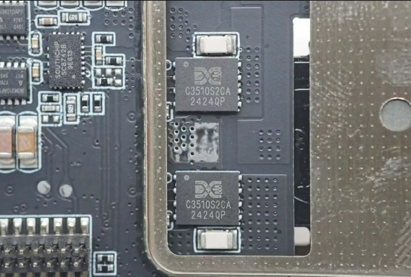
So far, Nixi has rolled out two GaN PIIP chip models, namely DXC3510S2CA and DXC3510S3CA, both of which are tailored for high-demand scenarios including USB charger, wall charger and GaN charger manufacturing. Both chips have a voltage resistance of 100V, with on-resistances of 12mΩ and 4mΩ respectively. Their detailed parameters are elaborated below, along with their targeted applications in GaN charger and USB charger systems.
DXC3510S2CA
DXC3510S2CA is a 100V GaN PIIP chip that integrates a 100V E-mode GaN HEMT (with an on-resistance of 12mΩ) and a GaN gate driver. It is optimized for the design of high-efficiency and high-density power supplies, especially for USB charger and GaN charger products that require miniaturization and high power. The device features a wide input voltage range of 0~20V, enabling it to adapt to complex voltage fluctuation environments common in wall charger usage scenarios. Meanwhile, it supports ultra-high switching frequency, which significantly boosts system power density and response speed— a key advantage for GaN charger devices to achieve fast charging without overheating.

Thanks to the inherent advantages of GaN materials, DXC3510S2CA can achieve fast and controllable rise time, optimizing switching loss and improving energy efficiency. For USB charger and wall charger products, this means lower energy consumption and longer service life. In addition, its zero reverse recovery loss characteristic completely solves the energy waste problem of traditional silicon-based devices during freewheeling, which has long been a pain point for low-efficiency wall charger and ordinary USB charging equipment. It is particularly suitable for circuit applications including high-frequency switching power supplies for GaN charger devices, synchronous rectification in USB charger systems, high-frequency DC-DC converters for wall charger products, motor drives, and class-D audio amplifiers.
DXC3510S3CA
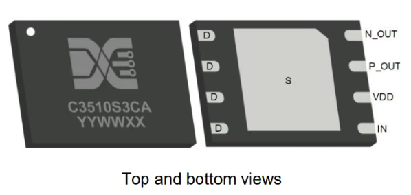
DXC3510S3CA is another GaN PIIP chip from Nixi Technology, and it has become a preferred chip solution for high-power GaN charger and USB charger manufacturers. Packaged in DFN 5×6, it integrates a 100V enhancement-mode GaN HEMT and a driver, with an on-resistance of 4mΩ— a lower resistance that brings more stable current output for wall charger and GaN charger products. Similar to DXC3510S2CA, this device also has a wide input voltage tolerance of 0~20V, making it adaptable to complex voltage fluctuation conditions in household and commercial USB charger scenarios. It also supports ultra-high switching frequency, which effectively enhances system power density and response speed, ensuring that GaN charger products can deliver fast charging while maintaining low temperature rise.

Benefiting from GaN material properties, DXC3510S3CA also realizes fast and controllable rise time, reduces switching loss and improves energy efficiency, which is crucial for reducing the heat generation of wall charger and USB charger devices during long-term use. Moreover, its zero reverse recovery loss feature eliminates the energy waste of traditional silicon devices in freewheeling, further improving the energy conversion rate of GaN charger products. It is ideal for applications such as high-frequency switching power supplies for GaN charger systems, synchronous rectification in USB charger circuits, high-frequency DC-DC converters for wall charger equipment, motor drives, and class-D audio amplifiers.
Summary from ChargerLab
Nixi’s GaN PIIP low-voltage GaN chips simplify peripheral circuits and cut costs effectively by virtue of their high integration and high-frequency switching characteristics, which is a boon for USB charger, wall charger and GaN charger manufacturers looking to balance performance and production costs. Compared with traditional low-voltage MOS solutions, GaN PIIP chips have lower switching loss and better temperature rise performance, which can effectively reduce system heat dissipation requirements for GaN charger and wall charger products, decrease parasitic inductance, optimize switching noise, and enhance product reliability. For USB charger devices, this translates to more stable charging current and safer usage experience, while GaN charger products can further expand their power range without sacrificing portability.
About Nixi Technology
Founded in April 2019, Nixi Technology is a high-tech enterprise led by an overseas returnee team, jointly established with top professors from the University of Electronic Science and Technology of China and industry elites. Headquartered in Nanjing, the company has collaborated with the ICiSC platform to build a national-level integrated circuit reliability testing platform. It is committed to developing a full-domestic GaN product line and providing high-performance and high-reliability solutions for new energy and national advanced basic industries, including core chips for USB charger, wall charger and GaN charger products.
Since its establishment, Nixi Technology has focused on the R&D and sales of GaN products, with a key focus on chips for charging devices such as GaN charger, USB charger and wall charger. Supported by its R&D and marketing centers in Chengdu and Shenzhen, it has formed a complete layout covering technology R&D, product testing, and market services, continuously promoting the innovation and application of GaN technology in the USB charger and GaN charger industries, and helping domestic wall charger manufacturers upgrade their product performance to compete in the global market.


 Infineon Launches 7 CoolGaN™ G5 700V Enhancement-Mode GaN Power Devices for Consumer Electronics


