


How Phone Charger Companies Improve User Experience and Device Safety?
 09 Mar,2026
When evaluating power electronics, phone charger companies face strict physical constraints regarding power density and thermal dissipation. Selecting the right architectural topology dictates not only charging speed but also the entire lifecycle safety of consumer electronics. Procurement decisions at this level require a deep understanding of component behavior under stress.
A proficient cell phone charger supplier understands that actual user experience extends far beyond mere peak wattage. It relies heavily on precise Ripple Control, robust fault protection mechanisms, and efficient switching frameworks. This article dissects the engineering realities and design choices behind industrial-grade charging systems.
Why Phone Charger Companies Prioritize Technical Fundamentals
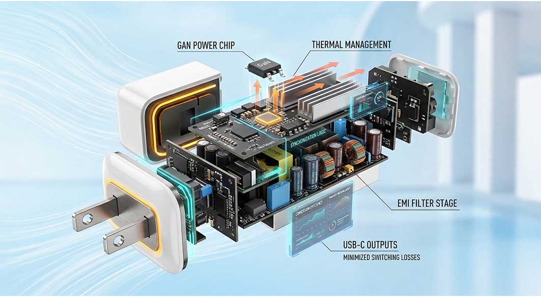
Modern fast-charging architectures demand meticulous attention to component-level interactions. Reputable phone charger factory focus heavily on conversion Efficiency, as any wasted electrical energy immediately translates into heat. The industry shift from silicon mosfets to Gallium Nitride (GaN) devices has fundamentally altered our approach to power density and thermal limits.
By leveraging high-electron-mobility transistors (HEMTs), power engineers can push switching frequencies significantly higher while minimizing switching losses. However, this high-frequency operation introduces severe new challenges in electromagnetic interference (EMI) filtering. Common-mode noise must be aggressively suppressed to pass global regulatory standards.
Properly designing the primary side controller to synchronize with secondary synchronous rectification is absolutely critical. If dead-time optimization is ignored during the design phase, destructive cross-conduction occurs, leading to immediate catastrophic failure.
This technical reality emphasizes why a generic reference circuit design is insufficient for high-demand consumer applications. It requires rigorous Validation and comprehensive Failure Mode Analysis during the early PCB prototyping stages to ensure commercial viability.
Overcoming Industry Pain Points: A Challenge for Phone Charger Factory
The B2B power supply market is currently plagued by over-promised specifications and under-delivered continuous reliability. A major industry pain point is thermal runaway in ultra-compact charger designs. Many low-cost alternatives achieve their rated maximum output for only a few minutes before thermal throttling severely degrades the charging current.
Another critical electrical issue is poor voltage ripple control on the DC output. High peak-to-peak ripple continuously stresses the smartphone's internal power management IC (PMIC), drastically accelerating battery aging. When evaluating a cell phone charger supplier, procurement managers must look beyond marketing claims and analyze oscilloscope data.
A lack of comprehensive Over-Voltage Protection (OVP) and Over-Current Protection (OCP) further jeopardizes connected device safety. In transient load conditions, lagging feedback loops can cause momentary voltage spikes that permanently damage sensitive logic boards.
Engineering Trade-off Analysis: The Reality of Design Constraints
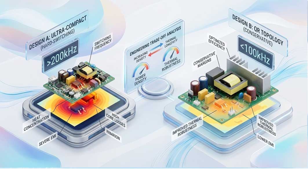
In power electronics engineering, there are no perfect solutions, only optimized trade-offs tailored to specific applications. A common misconception among buyers is that maximizing Switching Frequency Optimization automatically yields the best overall product. While higher frequencies shrink magnetic components, they drastically increase core losses and exacerbate EMI emissions.
Some suppliers intentionally push switching frequencies beyond 200kHz to achieve an ultra-compact form factor, simply because it "looks better" on a spec sheet. However, without utilizing expensive zero-voltage switching (ZVS) topologies like Active Clamp Flyback (ACF), this choice destroys overall efficiency and causes severe heat concentration in B2B applications.
The engineering trade-off here is strictly between volumetric power density and thermal robustness. For long-term continuous operation, choosing a slightly larger quasi-resonant (QR) topology with conservative thermal margins often provides a significantly higher Mean Time Between Failures (MTBF) than pushing a high-frequency hard-switching design to its absolute thermal limits.
Implementation of Advanced Topologies and Ripple Control
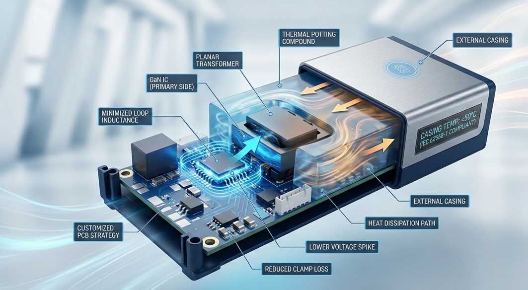
Translating theoretical schematic models into mass-producible physical designs requires strict adherence to mechanical and thermal constraints. Addressing high-density thermal bottlenecks involves highly specific component selection and customized PCB layout strategies to minimize loop inductance.
For example, in addressing the skin effect and proximity effect within high-frequency magnetics, the Tommox engineering framework utilizes planar transformers integrated with primary-side GaN ICs to reduce parasitic inductance and minimize leakage energy.
This specific engineering choice physically reduces the voltage spike on the primary switch during the turn-off phase. Consequently, it lowers the required clamping circuit dissipation, allowing the internal thermal energy to be distributed more evenly across the external casing.
By employing advanced potting compounds, the thermal resistance from the internal hot spots to the external ambient environment is significantly reduced. This ensures the casing temperature remains strictly within the IEC 62368-1 safety touch limits under continuous full-load testing.
Specification & Approach Comparison for B2B Buyers
To make an informed commercial decision, technical sourcing managers must evaluate the core architectural differences. Understanding these engineering variables separates reliable phone charger companies from low-tier generic assemblers.
Topology Selection: ACF provides superior efficiency and high density but requires complex, expensive control ICs. QR Flyback offers excellent cost-effectiveness and proven reliability for standard-sized chargers.
Thermal Management: Relying solely on air convection is insufficient above 45W. Robust designs utilize high thermal conductivity potting glue (>1.2 W/m·K) to pull heat away from the main transformer and switching nodes.
Protocol Compatibility: Modern IC solutions must support Programmable Power Supply (PPS). This allows dynamic voltage stepping in 20mV increments, enabling direct smartphone charging and reducing heat generation inside the phone itself.
Component Derating: A reliable cell phone charger supplier applies at least a 20% voltage derating rule for primary electrolytic capacitors to ensure longevity under severe utility grid fluctuations.
Future Trends & Design Direction
The trajectory of consumer and industrial power supplies is aggressively moving toward multi-protocol integration and absolute physical miniaturization. We are currently witnessing a rapid adoption of digital controllers replacing traditional analog feedback loops across all wattage tiers.
This digital shift allows for much more sophisticated dynamic power allocation when multiple high-drain devices are connected simultaneously. Furthermore, wide-bandgap (WBG) materials will continue to evolve, pushing power boundaries further.
For B2B buyers looking to future-proof their procurement catalogs, partnering with a highly technical [Custom Multi-Port Fast Charging Solutions] provider is essential. The industry focus must remain clearly on the intersection of firmware intelligence and hardware durability.
FAQ for Sourcing Managers Selecting a Cell Phone Charger Supplier
Q1: How does an excessive output ripple affect the end user's device?
Excessive ripple causes micro-heating within the device's battery management system (BMS). Over an extended period, this thermal stress accelerates lithium-ion cell degradation and can cause touchscreen ghosting or erratic input during charging.
Q2: Why do some high-wattage chargers fail thermal compliance testing?
Many generic designs lack adequate Thermal Management systems. They rely on cheap thermal pads rather than full-potting structural solutions, causing internal hot spots that eventually trigger thermal shutdown or premature component failure.
Q3: What should we look for in the bill of materials (BOM) when auditing phone charger companies?
Prioritize the quality and brand of the primary bulk capacitor, the specific type of GaN IC used (integrated driver vs. discrete mosfet), and the presence of dedicated synchronous rectification controllers on the secondary side.
Q4: Is Active Clamp Flyback (ACF) always necessary for PD chargers?
No. ACF is typically mandatory for ultra-high-density designs (above 1.2W/cc). For standard-size chargers where volumetric thermal constraints are looser, an optimized QR topology often provides better commercial cost-efficiency and comparable MTBF.
 Top 5 Factors to Consider When Sourcing Wholesale USB-C Chargers from a PD Charger Factory