



Samsung 60W Zero Standby Power GaN Charger (EP-T6010) Full Review & Teardown
 26 Aug,2026
Introduction
This article presents a comprehensive review and full teardown of the Samsung EP-T6010 60W GaN fast charger, a flagship power adapter tailored for Samsung’s 2025 and subsequent flagship smartphone models. Distinguished from conventional gallium nitride chargers, this device integrates two core advantages: mature GaN semiconductor technology for efficient fast charging and industry-leading zero standby power consumption.
Built upon the Joulwatt BP87650A and BP62650A dual-chip power solution with patented magnetic coupling communication components, the charger achieves an ultra-low standby power consumption below 2mW, far exceeding the IEC62301 international standard for zero standby power (below 5mW). It also fulfills Samsung’s long-term energy efficiency commitment, setting a new benchmark for high-power charger energy-saving design in the consumer electronics industry.
Unboxing & Exterior Design
Packaging Overview
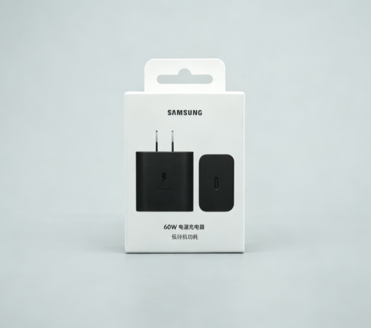
The charger adopts Samsung’s classic packaging design style, with the front side printed with the SAMSUNG brand logo, official product name, and product appearance renderings. The back of the package clearly displays complete product parameters, manufacturing date, packaging contents, and safety prompt information. The standard package includes the 60W GaN charger, three-pack warranty certificate, and hazardous substance list, delivering a standardized and formal user experience.
Body Appearance & Craftsmanship
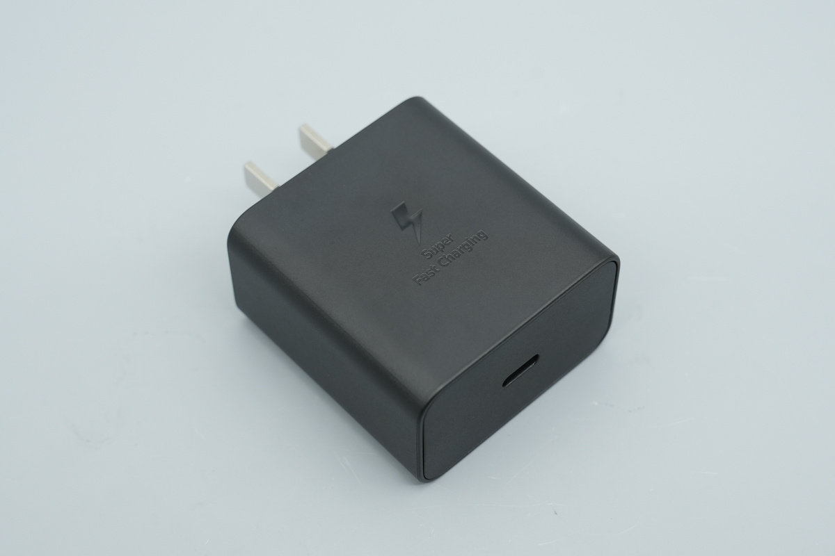
The charger features an all-black body with a matte anti-fingerprint finish, ensuring comfortable hand feel and effective resistance to daily smudges and scratches. The front center is engraved with Samsung’s classic lightning icon and the “Super Fast Charging” slogan, highlighting its fast charging positioning. The side of the body is marked with “60W” power rating and “Low Standby” low-power identification, directly presenting its core product features.
Equipped with a national standard foldable plug and a single middle-positioned USB-C port on the top, the charger boasts a compact and integrated structural design. Its precise dimensional measurements are 48.08mm in length, 46.13mm in width, and 28.11mm in thickness, with a net weight of approximately 103g. Compared with the Apple 67W charger, it achieves a more miniaturized body size while maintaining equivalent power, offering superior portability.
Core Parameter & Protocol Compatibility
Official Hardware Parameters
Modeled EP-T6010, this charger supports a global universal input voltage of 100-240V~50/60Hz 1.6A, adapting to power supply standards in various regions worldwide. It delivers two mainstream output modes: PDO fixed voltage output and PPS adaptive voltage output. The PDO mode covers 5V3A, 9V3A, 15V3A, and 20V3A gears, while the PPS mode supports 5-20V3A wide-range adjustable output, realizing 15-60W full-power dynamic output. Additionally, the product has passed CCC certification and Level VI energy efficiency certification, meeting international mainstream safety and energy-saving standards.
Charging Protocol Support
Actual testing verifies that the USB-C port of the charger is compatible with multiple mainstream fast charging protocols, including PD3.0, PPS, QC5, and DCP. The PDO message detection confirms four fixed voltage gears and three sets of PPS flexible voltage gears (5-11V5A, 5-16V4A, 5-21V3A), enabling adaptive matching of fast charging solutions for Samsung flagship devices and most mainstream Android smartphones, tablets, and digital devices on the market.
Key Performance Test & Zero Standby Power Verification
Flagship Device Charging Power Test
In the actual charging test for Samsung Galaxy S26 Ultra flagship phone, the charger maintains a stable peak charging power of 51.54W, fully meeting the fast charging demand of Samsung’s new-generation flagship devices and ensuring efficient power replenishment.
Ultra-Low Standby Power Test
Zero standby power is the core technological highlight of this product. Based on the IEC62301 standard that defines standby power below 5mW as zero standby, the charger shows excellent low-power performance in dual-voltage environment tests. Under 110V input, the no-load standby power consumption is only 1.23mW; under 220V conventional household voltage input, the standby power consumption is merely 1.8mW. Both test results are far below the international standard threshold, reserving sufficient energy efficiency upgrade space for subsequent high-power charging products.
In-Depth Internal Hardware Teardown
Overall Structural Design
The charger shell adopts ultrasonic welding encapsulation process with high structural tightness. The internal PCBA module is filled with thermal conductive glue and wrapped with integrated heat dissipation copper sheets, realizing efficient heat conduction and passive heat dissipation. The inner wall of the shell is pasted with high-temperature resistant insulating tape and copper foil, with multi-layer insulation and heat dissipation designs on all sides to ensure operational safety and stability. The plug is connected through contact power-on and crimped with metal sheets for reliable power input.
The measured dimensions of the internal PCBA module are 44.45mm in length, 42.81mm in width, and 23.66mm in thickness. The overall layout is compact and orderly, with independent isolation designs for primary and secondary circuits, and plastic shell reinforcement for the USB-C interface seat to enhance drop resistance and durability.
Front-end Input Circuit Components
The input circuit is equipped with a complete EMI filtering and overcurrent protection system. A 2A 250V delay fuse from Better Electronics is deployed for overcurrent safety protection. Dual common-mode inductors and differential-mode inductors are configured to effectively filter high-frequency electromagnetic interference and ensure stable and pure input current. The rectifier bridge adopts RULBF810T model to realize efficient AC-DC rectification conversion.
High-voltage filter electrolytic capacitors are all supplied by CapXon, including one 400V 27μF and three 400V 18μF specifications, which fully filter high-voltage ripples and stabilize the primary circuit voltage. The rectifier plate is attached with thermally conductive ceramic sheets on both sides to assist heat dissipation and reduce component operating temperature.
Core Control & Power Device Configuration
The entire power system adopts Joulwatt’s exclusive low-power dual-chip solution. The primary side is equipped with BP87650A quasi-resonant flyback controller, which integrates a high-efficiency GaN gate driver, 700V high-voltage start-up current source, and multi-functional protection circuit. Cooperating with the patented BP818 magnetic coupling communication element without bias current loss, it realizes ultra-low power consumption operation in standby mode. The secondary side matches the BP62650A dedicated secondary controller, which adopts ripple-based adaptive control algorithm, eliminating complex loop compensation circuits and supporting ultra-low power sleep in standby state.
The high-performance GaN power switch adopts Navitas NV6015C chip, with 150mΩ on-resistance, 700V withstand voltage (supporting 800V transient overvoltage), and up to 10MHz switching frequency. It features ultra-low gate charge and zero reverse recovery charge, greatly reducing switching loss and improving overall conversion efficiency. The synchronous rectifier device adopts SemiHow HRLF69N10 to optimize rectification efficiency.
Protocol & Output Circuit Design
The fast charging protocol is undertaken by Joulwatt BP63430N highly integrated controller, which complies with USB PD3.1 latest standard and supports mainstream protocols such as BC1.2, QC series, and UFCS, with customizable private protocol functions. Built-in 32-bit processor, 12-bit ADC and DAC ensure accurate voltage and current regulation and fast transient response.
The output circuit is equipped with two CapXon 28V 390μF solid-state filter capacitors to eliminate output ripples and ensure stable voltage output. The VBUS switch tube adopts high-reliability DFN3*3 packaged device, with fast response speed and strong overcurrent protection capability. Meanwhile, TMY1101K patch Y capacitor from Terui Xiang is configured to optimize EMC performance and meet global safety certification standards.
Product Advantages & Market Positioning
As Samsung’s new-generation flagship fast charging adapter, the EP-T6010 achieves a perfect balance of efficiency, energy saving and portability. Its biggest advantage lies in the breakthrough zero standby power technology, which far surpasses industry average energy efficiency levels and effectively reduces idle power consumption, conforming to global energy-saving and low-carbon development trends. The mature GaN power device ensures high conversion efficiency and low heat generation during high-power charging.
In terms of compatibility, full coverage of mainstream fast charging protocols enables it to serve not only Samsung flagship devices but also most mainstream digital products. The compact miniaturized design and complete safety certification make it an ideal travel and daily charging adapter, leading the upgrading direction of high-power and low-energy-consumption charging equipment in the consumer electronics industry.
 Lenovo USB PD 3.1 GaN Charger Series: Full Specs, Protocols & Use Case Comparison