


Innoscience Launches Five 150V Low-Voltage GaN Products
 17 Nov,2025
Since gallium nitride (GaN) entered the consumer fast-charging market, it has achieved breakthroughs in charger power density and efficiency凭借 its high breakdown field strength, low on-resistance, and high-speed switching characteristics. The product volume has been reduced by more than 50% compared to silicon-based solutions, making it the core solution for "small-sized fast chargers" such as compact wall chargers and USB-C chargers. However, unlike the popularity of high-voltage GaN in the AC-DC field, low-voltage GaN has previously been restricted by factors such as cost and drive compatibility, leading to slow progress in large-scale applications.
In recent years, with the improvement of production capacity and ecosystem, low-voltage GaN has ushered in a development inflection point. Innoscience has顺势布局 a 150V grade low-voltage GaN device matrix, injecting new vitality into high-frequency power supply applications through multi-dimensional technological breakthroughs.
Key Highlights of Innoscience 150V Low-Voltage GaN Products
Innoscience has now launched five 150V low-voltage GaN single tubes, with on-resistance covering 3.9~7mΩ, and providing three packaging forms: FCQFN, En-FCQFN, and LGA, to adapt to the needs of different application scenarios including wall chargers and USB-C chargers.
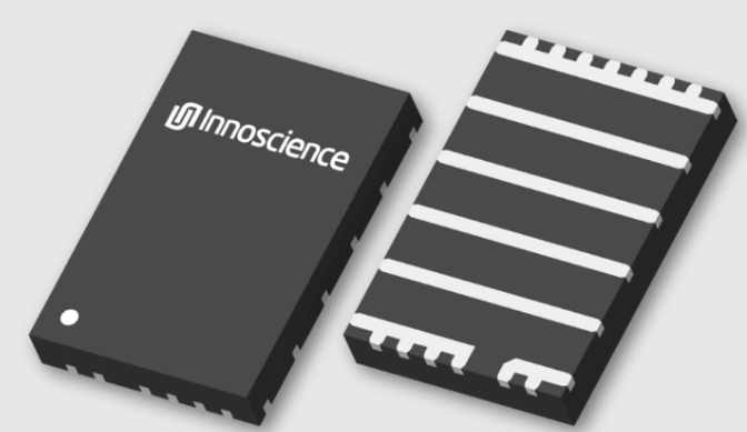
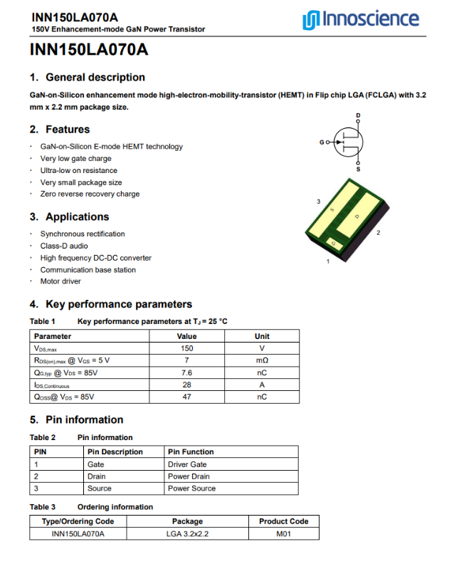
INN150LA070A: Silicon-based GaN, adopting FCLGA 3.2×2.2 package, with on-resistance as low as 7mΩ, low loss in high-frequency and high-efficiency scenarios. Zero reverse recovery charge brings better EMI performance, suitable for synchronous rectification, Class-D audio, PD fast charging, high-frequency DC-DC converters and other fields related to USB-C chargers.
INN150EQ032A: 150V enhancement-mode silicon-based GaN, compact En-FCQFN 4×6 package, with 3.9mΩ on-resistance and low gate charge, excellent power conversion efficiency, which can effectively reduce system loss and volume. Its application scenarios include synchronous rectification, PD fast charging, communication base stations, motor drives and wall charger designs.
INN150FQ070A/INN150EQ070A: Both are 150V silicon-based GaN with 7mΩ on-resistance, adopting FCQFN 4×6 and En-FCQFN 4×6 packages respectively. They have the advantages of low gate charge, ultra-low conduction loss and small package size, suitable for high-frequency DC-DC conversion, telecommunication power supplies, solar micro-inverters and other scenarios including USB-C charger manufacturing.
Currently, low-voltage GaN is accelerating from demonstration applications to the mainstream market. Relying on low conduction loss, high switching frequency and compact packaging, it has widely penetrated into multiple fields such as PD fast charging, car chargers, motor drives, wall chargers and USB-C chargers. With the steady increase in production capacity of 8-inch wafer production lines, the penetration rate of low-voltage GaN in next-generation electronic products will continue to accelerate in the future.
 Huawei Opens 66W Fast Charging Authorization – Third-Party USB Chargers Offer Factory